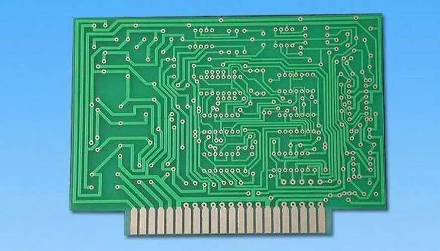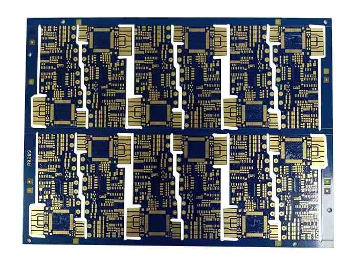
Two alternate 4-layer PCB stacks with 50 ohm impedance
New designers upgrading from 2-layer to 4-layer boards may be ready to start using power and ground planes, and most manufacturers will provide standard stacks to help you build your design. You often see that the recommended basic layer is a SIG/GND/PWR/SIG type layer, where the inner layer is a plane or a large polygon. For many types of designs, as long as you don't make some simple layout and routing mistakes.
If you need to perform more advanced operations, such as placing and routing high-speed components on both sides of the circuit board, you need to use alternate layers. Typical wiring errors that lead to basic 4-layer stacking involve wiring high-speed signals between surfaces without providing a clear return path, resulting in a large amount of radiated EMI from the circuit board. Instead, you should create your PCB stack and layout using one of these alternative 4 layers.
Stack # 1: GND/SIG+PWR/SIG+PWR/GND
The outer layer of the stack is grounded to provide high shielding to external EMI. It can also provide a good simple path for ESD to return to GND and finally return to the equipment chassis or grounding, without following the path through the through-hole to the internal layer. From the perspective of EMI and ESD, this type of design, with the outer layer grounded and low impedance directly connected to GND, is definitely the safest design. If necessary, it can also be well extended to higher levels.
This stack provides a high shielding of external noise, but has little effect on suppressing the internal noise (crosstalk) between high-speed signals on different layers.
The potential problem with this stack is crosstalk between signals on different layers. Normally, the thick core in the circuit board is about 40 mils, but this is not necessarily enough to ensure that the routing will not receive crosstalk, especially at high speeds. The best way to prevent inductance crosstalk is to use orthogonal wiring on different layers. In addition, do not use it for high speed signals or high frequencies, otherwise you may see capacitive crosstalk between signal layers (especially at high power GHz frequencies).

To eliminate crosstalk problems, consider reversing this stack as shown below.
Stack # 2: SIG+PWR/GND/GND/SIG+PWR
For me, this stack is preferable, especially for any circuit board that needs to transmit high-speed signals between two surface layers of the circuit board. This stack is just the inversion of the previous stack. However, its functions are different, which does not necessarily mean that it provides a high degree of isolation from external noise sources. On the contrary, it is a better choice for systems that require high-speed components and wiring on both sides of the circuit board. It is also easy to design this 4-layer stack for a 50 ohm control impedance. Finally, make sure that the GND plane is connected to the adjacent vias wherever the signal conversion takes place. PCB design and PCB processing manufacturer's explanation: two alternative 4-layer PCB stacks with 50 ohm impedance.
In the SIG+PWR/GND/GND/SIG+PWR stack, the digital return current in the PWR plane may return to ground along a very large loop. One path is through the nearest de capacitance, but this does not eliminate low frequency EMI.
The tradeoff of this stack is that the shielding of external signals is low. The signals on each side of the circuit board are shielded from each other, but are not affected by external radiation sources. Another advantage of this stack is that you can route directly into components without cutting the ground plane. In general, compared with the standard SIG/PWR/GND/SIG stack, these advantages of this stack and the previous stack are very suitable for high-speed design of cabling on two surfaces.
Why are these stacks more suitable for single ended high-speed signals
The standard SIG/PWR/GND/SIG lamination of 4-layer boards is still applicable to high-speed, but you can only reliably support medium to high-speed numbers on one side of the board. This is because the SIG/GND layer is very suitable for digital signals; The signal layer adjacent to the GND layer is the layer that should be used for digital, for the following reasons:
Controlled impedance: The close spacing between GND layer and SIG layer allows you to define the controlled impedance single ended routing as 50 ohms (or some other impedance) without making the routing too wide.
Shielding: The SIG+PWR/GND/GND/SIG+PWR stack has the highest shielding capacity for internal noise and interlayer crosstalk, while the reverse stack has the highest shielding capacity for external noise. However, if the wiring is incorrect, internal crosstalk will occur
Clear return path: The capacitive coupling return path has low impedance because it is directly excited in the ground plane. This is compared with the SIG/PWR layer pair, which presents a high impedance return path or a very large return current loop that generates EMI.
You will see that the biggest reason for using one of these alternative stacks is the last point in this list, and you need to provide a return path. The return path sensed in the power plane is unpredictable and can be very large.
In the SIG/PWR/GND/SIG stack, the digital return current in the PWR plane may return to ground along a very large loop. One path is through the nearest de capacitance, but this does not eliminate low frequency EMI.
To try to reduce the loop area and impedance of the digital signal return path, a Band Aid may be placed on the surface layer around the wiring above the power plane. However, the capacitive coupling between the cabling and the signal may be weak, and it cannot guarantee a significant reduction in EMI.
Although you have only one ideal digital signal layer instead of two, the standard SIG/PWR/GND/SIG stack has other advantages. With a dedicated power plane, you can still route higher currents than the copper cladding used to route power; This is very useful in power systems that require some digital control circuits. The back layer can be used to fix various other components, such as connectors or passive components.
The important points of a standard 4-layer stack design, especially when placing power in a 4-layer circuit board, are as follows: Including a dedicated power layer will not cause your design to automatically pass the EMC test. However, just because you are wiring on a unified power plane, do not assume that you can wire your digital signals at will. It is more important to understand how the return path propagates in the power plane and how it is ultimately coupled back to the ground through a high impedance return path.
No matter what type of 4-layer PCB stack you want to build, the design tools you use can help you quickly customize the stack and create your PCB layout. Both can create schematics, PCB layouts, and manufacturing documents needed to transform design from conception to production.


