Never cross the ground plane gap in high-speed PCB design
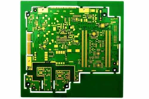
Make sure that these lines do not cross the ground level gap
I often browse electronic products and PCB forums, and I see that I ask the same question again and again: Why should I not wire on the crack in the ground plane? Everyone from manufacturers to professional designers just dabbling in high-speed PCB design will ask this question. For professional signal integrity engineers, the answer should be obvious.
Whether you are a long-term PCB layout engineer or a temporary designer, it is helpful to understand the answer to this question. The answer is always framed as always/never stated. I usually don't like to give absolute answers to PCB design questions, but in this case, the answer is clear: never route the signal to the gap on the ground plane. Let's take a closer look at why we should not route on gaps in the ground plane.
Ground clearance: low speed and high speed design
To answer this question, you need to consider the performance of the signal under DC, low speed and high speed. This is because each type of signal will generate a different return path in the reference plane. The return path your signal follows will have some important effects on the EMI generated in the circuit board and the sensitivity of specific circuits to EMI.
If you understand how the return current in a PCB is formed, it is easy to understand how it affects EMI and signal integrity. This is why it is important - it is related to the wiring on the ground plane gap. The circuit formed by the return current in the circuit board determines two important behaviors:
EMI sensitivity. The loop generated by the power supply and return current in the circuit determines the sensitivity of the circuit board to EMI. Circuits with large current loops will have larger parasitic inductance, making them more vulnerable to radiated EMI.
The switch signal rings. When the signal switches between levels, the parasitic inductance in the circuit determines the damping level of the transient response in the circuit. When used with parasitic capacitors in the circuit, these two quantities determine the natural frequency of the transient response and the damped oscillation frequency.

Let's look at DC, low speed and high speed signals in detail:
DC voltage/current
When the circuit board operates with DC power supply, return current will not be generated directly under the signal wiring; It will follow a straight line back to the supply return point. This means that you basically cannot control the return path, and because of the large parasitic inductance, the circuit board may be vulnerable to EMI. Some people may think that there will be no transient oscillation because the power supply is not switched, so it does not matter whether the microstrip line runs through the ground plane gap. Although there is no oscillation, the problem of EMI sensitivity still exists. You should try to keep the inductance of the DC circuit as low as possible. The best way to reduce the inductance of the circuit is to avoid wiring through the ground plane gap.
Low speed signal
Just like the DC signal, the return path determines the loop inductance of the circuit, which determines the EMI sensitivity and damping in the transient response. If the loop inductance is large, the damping rate will be low. As in the case of DC signals, wiring through the ground plane gap will increase the loop inductance, thus affecting signal integrity, power integrity and EMI.
Unfortunately, low speed signals have become history, and every circuit board that uses TTL and faster logic will behave as a high speed circuit. For low-speed signals (typically 10 ns rise time or slower), the ringing amplitude in a particular circuit is usually low enough not to be noticed. Therefore, as long as the signal is not routed through the ground plane gap, the loop inductance is usually low enough to prevent strong ringing, EMI sensitivity, and related power integrity issues.
High speed signal
If I use a circuit board designed for low speed operation and run it with a high speed signal, the ringing amplitude will be greater for a given circuit loop inductance. Again, this means that the loop inductance in the circuit board needs to be kept as small as possible. The goal is to provide as much damping as possible to reduce the ringing amplitude in a given interconnect. Similarly, wiring through ground plane gaps will avoid increasing loop inductance. In addition, the grounding plane should be placed below the signal layer carrying high-speed circuits to ensure that the loop inductance in the entire interconnection is as low as possible.
An example return path for signals routed through the ground plane gap.
Another way to view the ground plane gap is impedance discontinuity. If the signal is routed through the ground plane gap, the impedance of the area above the gap will be greater than the impedance of the rest of the interconnect. In addition to the above aggravated ringing problem, this can also cause signal reflection.
Learn more about high-speed signal transmission on ground plane gaps.
Everything about digital signals mentioned above applies equally to analog signals. The transient signal problems mentioned above are related to power integrity problems, especially in circuit boards that use high gate/pin count components. The layer stack should be specifically designed to support faster than TTL components (see below).
Clearance between power rail and ground plane
Note that we have studied this from a signal integrity perspective, but the same idea applies to power integrity. Just as microstrip routing should not cross the ground plane gap, you should also avoid routing power rails on the surface layer above the ground plane gap. If you provide DC power for the digital IC, it will draw some current from the power supply when the IC switches between ON and OFF states. This will create a voltage ripple on the power rail.
This special transient response in the power supply voltage is characterized by damped oscillation. Its amplitude is proportional to the impedance of PDN and inversely proportional to the damping level in PDN. Just as damping is inversely proportional to the loop inductance in a standard PCB interconnect, this also applies to transient responses in PDNs. This means that if the loop inductance is kept small, the transient response on the power rail can be suppressed. The best way to do this is to place the ground plane on a layer directly adjacent to the power plane and avoid wiring any power rails on any ground plane gap.
If you are using a two-layer board and there is no space to place a ground plane, you should carefully plan the return path in the board to maintain a small loop inductance. One option is to use grid arranged grounding areas at the top and bottom layers and connect them through vias. However, if you are processing high-speed signals (TTL and faster), you will see large voltage fluctuations on the power rail due to insufficient capacitance in the PDN. This is the main reason why the power and ground planes in high-speed circuit boards are placed on adjacent layers, while the ground plane is placed directly below the signal/component layer. The circuit board assembly and circuit board processing manufacturers explained that they should never cross the ground plane gap in high-speed PCB design to ensure that these lines do not cross the ground plane gap.


