Ten Rules of Efficient and Effective PCB Design Process
Prototype design and product development are very important in PCB design process. In order to make the PCB run normally and manufacture effectively, the following conditions need to be met:
Rule 1: Get the correct grid.
Find the grid spacing that fits as many components as you can, and use it throughout the process. Although multiple grids may seem attractive, some additional consideration in the early stages of layout can avoid spacing difficulties and maximize the use of circuit boards. Many devices have different package sizes, so make full use of them. In addition, because polygons are important shapes when adding copper to boards, and boards with multiple meshes often have polygon filling differences, it will make your life more difficult if you do not standardize one mesh.
Rule 2: The length of routing should be as short and direct as possible
This rule applies even if it means re traversing parts of the layout to optimize the track length. This is particularly true for analog and high-speed digital circuits, where impedance and parasitic effects will always play a role in limiting system performance.
Rule 3: Use the power plane as much as possible to manage the distribution of power lines and ground.
In most PCB design software, pouring on the power board is a quick and easy choice. It uses a lot of copper on the common connection and helps to ensure that power flows as efficiently as possible with the minimum impedance or voltage drop, and that the ground loop is adequate. If possible, lay multiple power lines in the same area of the circuit board. Remember that if the ground plane extends over a large part of a layer, it may have a positive impact on the crosstalk between power lines above adjacent layers.

Rule 4: Combine related components and test points.
For example, the discrete components required by the operational amplifier are placed close to the device so that the bypass capacitor and resistor are co located with the device. This helps track length in Rule 2 and makes testing and fault finding easier.
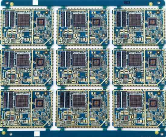
Rule 5: Panel a PCB by copying the required board on a larger board.
Using the size of the equipment most suitable for the manufacturer will increase prototype and manufacturing costs. First lay out the board as a panel. Ask your board members which panel size they prefer. Then, after correcting the design rules, try your best to step and repeat the design several times within the preferred panel size.
Rule 6: Merge your component values.
As a designer, you will choose some discrete components, which may have higher or lower value and work in the same principle. Merging a smaller range of standard values can make the BOM simpler and potentially cheaper. In the long run, if you configure a series of PCB boards according to your preferred device values, it will also make inventory decisions easier.
Rule 7: Accept as much design rule checking (DRC) as possible.
The DRC function on PCB software takes some time, but checking during the process can save time for more complex designs, which is a good habit to adopt. Every layout decision is important, but DRC always puts the most important decision first.
Rule 8: Use screen printing wisely.
Screen printing can be used to describe a large amount of useful information to circuit board manufacturers and service or test engineers, installation procedures or equipment operators. Clear labels describing functions and test points are obvious, but the orientation of components and connectors should also be considered as far as possible. It is still a good habit for annotations to appear under your components after the board is assembled. The full use of screen printing on both sides of the board can simplify production and reduce rework.
Rule 9: Decoupling covers are not optional!
Do not attempt to optimize the design by avoiding power cord decoupling and believing in the absolute limits of the component data manual. Capacitors are cheap and sturdy; Take the time to adapt to them as much as possible, and remember Rule 6 – Use a range of standard values to keep the list clean.
Rule 10: Generate your own PCB manufacturing data and verify it before sending it out for manufacturing.
Most boards will be happy to do this for you, but if you first output your Gerber file and use a free viewer to verify its appearance, you can avoid misunderstanding. You may even get into glass fiber, resin and copper by mistake before they are permanently set incorrectly.
As circuit designs are increasingly shared, and internal teams increasingly rely on reference designs, we believe it is important to retain such basic rules in printed circuit design. Mastering basic knowledge means that developers can maintain flexibility, add value to their products, and obtain maximum benefits from each circuit board manufactured. Finally, anyone who is not familiar with circuit board design can improve their learning curve and self-confidence while "designing" basic knowledge. The PCB processing factory explains the ten rules of efficient and effective PCB design process, PCB design process and effective manufacturing.


