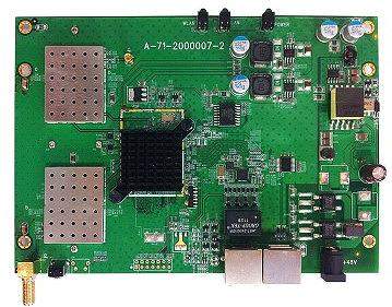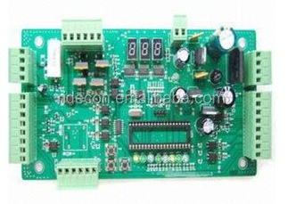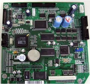
The names of circuit boards include: ceramic circuit board, alumina ceramic circuit board, aluminum nitride ceramic circuit board, circuit board, PCB board, aluminum substrate, high-frequency board, thick copper plate, impedance board, PCB, ultra-thin circuit board, ultra-thin circuit board, printed (copper etching technology) circuit board, etc. The circuit board makes the circuit miniature and intuitive, which plays an important role in the mass production of fixed circuits and the optimization of the layout of electrical appliances. The circuit board can be called a printed circuit board or a printed circuit board, and its English name is (Printed Circuit Board) PCB (Flexible Printed Circuit board) FPC circuit board (FPC circuit board is also called flexible circuit board. Flexible circuit board is a highly reliable and excellent flexible printed circuit board made of polyimide or polyester film. It has the characteristics of high wiring density, light weight, thin thickness, and good flexibility.) and soft and hard combination plate (reechas, soft and hard combination plate) - the birth and development of FPC and PCB, The birth of the soft and hard combination board this new product. Therefore, the soft and hard combination board is a circuit board with FPC characteristics and PCB characteristics formed by combining the flexible circuit board and the hard circuit board according to relevant process requirements after pressing and other processes.
Detailed analysis of basic knowledge of circuit board
classification

According to the number of layers, PCB can be divided into single panel, double panel, and multi-layer PCB.
First is the single panel. On the most basic PCB, parts are concentrated on one side and wires are concentrated on the other side. Because wires only appear on one side, this PCB is called single-sided circuit board. Single panel is usually simple to make and low in cost, but its disadvantage is that it cannot be applied to too complex products.
Double panel is an extension of single panel. When single-layer wiring cannot meet the needs of electronic products, double-sided panel will be used. Both sides are copper coated and wired, and the line between the two layers can be conducted through the via to form the required network connection.
Multilayer board refers to a printed board with more than three conductive graphic layers and insulating materials between them laminated at intervals, and the conductive graphics between them are interconnected as required. Multilayer circuit board (MLPCB) is the product of the development of electronic information technology in the direction of high speed, multi-function, large capacity, small volume, thin and lightweight.
PCB can be divided into soft board (FPC), hard board (PCB) and soft hard combination board (FPCB) according to characteristics.
PCB board
FR-1: fire-retardant copper-clad phenolic paper laminate. IPC4101 detailed specification No. 02; Tg N/A;
FR-4:1) Flame retardant copper clad epoxy E glass fiber cloth laminate and its adhesive sheet material. IPC4101 detailed specification No. 21; Tg≥100℃;
2) Flame retardant copper clad foil modified or unmodified epoxy E glass fiber cloth laminate and its adhesive sheet materials. IPC4101 detailed specification No. 24; Tg 150℃~200℃;
3) Flame retardant copper clad epoxy/PPO glass cloth laminate and its adhesive sheet materials. IPC4101 detailed specification No. 25; Tg 150℃~200℃;
4) Flame retardant copper clad foil modified or unmodified epoxy glass cloth laminate and its adhesive sheet materials. IPC4101 detailed specification No. 26; Tg 170℃~220℃;
5) Flame retardant copper clad epoxy E-glass cloth laminate (for catalytic addition method). IPC4101 detailed specification No. 82; Tg N/A;
Inspection and repair
I. Chip with program
1. EPROM chip should not be damaged generally. Because this chip needs ultraviolet light to erase the program, it will not damage the program in the test. However, it is reported that due to the materials used to make the chip, it may be damaged (mainly referring to the program) even if it is not used. So backup as much as possible.
2. EEPROM, SPROM, etc. and RAM chip with battery are very easy to damage the program. Whether this kind of chip destroys the program after VI curve scanning with<Tester>has not been determined. Nevertheless, colleagues should be careful when encountering such situations. The author has done many tests, and the possible major reason is that the shell of maintenance tools (such as tester, electric soldering iron, etc.) leaks electricity.
3. The chip with battery on the circuit board shall not be removed from the board easily.
II. Reset circuit
1. When there are large-scale integrated circuits on the circuit board to be repaired, pay attention to reset.
2. Before the test, it is better to install it back on the equipment, turn it on repeatedly and turn it off for a try. And press the reset key several times.
III. Function and parameter test
1.<Tester>The detection of devices can only reflect the cut-off area, amplification area and saturation area. However, it is impossible to measure the working frequency, speed and other specific values.
2. Similarly, for TTL digital chips, only high and low level output changes can be known. It is impossible to detect the speed of its rising and falling edges.
IV. crystal oscillator
1. Generally, the oscilloscope (the crystal oscillator needs to be powered on) or frequency meter can only be used for testing, and the multimeter cannot be used for measuring, otherwise the substitution method can only be used.
2. Common faults of crystal oscillator include: a. internal leakage, b. internal open circuit, c. deterioration frequency offset, d. leakage of external connected capacitors. The leakage phenomenon here can be measured with VI curve<tester>.
3. Two judgment methods can be used during the whole board test: a. Relevant chips around the crystal oscillator fail during the test. b. No other fault points were found except crystal oscillator.
4. There are two kinds of crystal oscillators: a. Two feet. b. Four pins, of which the second pin is powered on, please note that no random short circuit is allowed.
V. Distribution of fault phenomena
1. Incomplete statistics of circuit board fault location: 1) 30% chip damage, 2) 30% discrete component damage,
3) The connecting wire (copper wire on PCB board) is broken by 30%, 4) the program is damaged or lost by 10% (with an upward trend).
2. It can be seen from the above that when the circuit board to be repaired has wiring and program problems, and there is no good board, we are not familiar with its wiring and can not find the original program. It is unlikely that this board will be repaired.
Compatible design
EMC refers to the ability of electronic equipment to work coordinately and effectively in various electromagnetic environments. The purpose is to make electronic equipment not only suppress various external interference, so that electronic equipment can work normally in a specific electromagnetic environment, but also reduce the electromagnetic interference of electronic equipment itself to other electronic equipment.
1. Select a reasonable wire width. Since the impact interference caused by transient current on the printed lines of PCB is mainly caused by the inductance of the printed wire, the inductance of the printed wire should be minimized.
2. The correct wiring strategy and equal routing can reduce the conductor inductance, but the mutual inductance and distributed capacitance between the conductors increase. If the layout allows, it is better to use the well shaped network wiring structure. The specific method is that one side of the printed board is wired horizontally and the other side is wired longitudinally, and then connected with the metallized hole at the cross hole.
3. In order to suppress the crosstalk between the wires of PCB circuit board, long distance equal routing shall be avoided as far as possible during the design of wiring, the distance between lines shall be pulled as far as possible, and the signal line shall not cross the ground wire and power line as far as possible. A grounded printed wire is set between some signal wires that are very sensitive to interference, which can effectively suppress crosstalk.
form
The circuit board is mainly composed of pads, vias, mounting holes, wires, components, connectors, fillers, electrical boundaries, etc. The main functions of each component are as follows:
Soldering pad: It is used to weld metal holes of component pins.
Through hole: there are metal through hole and non-metal through hole, in which the metal through hole is used to connect the component pins between layers.
Mounting hole: used to fix the circuit board.
Wire: copper film of electrical network used to connect the pins of components.
Connector: components used for connecting circuit boards.
Filling: used for copper coating of ground wire network, which can effectively reduce impedance.
Electrical boundary: used to determine the size of the circuit board. All components on the circuit board cannot exceed this boundary.
Main classification
Circuit board systems are classified into the following three categories:
Single panel
Single-Sided Boards
We just mentioned that, so we call this PCB single sided. Because there are many strict restrictions on the design circuit of a single panel (because there is only one side, and the wiring cannot intersect with each other and must go around a separate path), only early circuits use such boards.
Double-sided board
Double-Sided Boards
This circuit board has wiring on both sides. However, if you want to use two wires, you must have a proper circuit connection between them. This "bridge" between circuits is called a pilot hole (via). The pilot hole is a small hole filled with or coated with metal on the PCB, which can be connected with the wires on both sides. Because the area of the double-sided board is twice as large as that of the single panel, and because the wiring can be staggered (it can be wound to the other side), it is more suitable for circuits more complex than the single panel.
Multilayer board
[Multilayer board] In case of complex application requirements, circuits can be arranged into multi-layer structures and pressed together, and through hole circuits can be arranged between layers to connect circuits of each layer.
Inner line
The copper foil substrate is first cut into a size suitable for processing and production. Before pressing the film on the substrate, it is usually necessary to roughen the copper foil on the plate surface by brush grinding, micro etching and other methods, and then attach the dry film photoresist to it with appropriate temperature and pressure. Send the substrate with the dry film photoresist to the ultraviolet exposure machine for exposure. The photoresist will polymerize after being exposed to ultraviolet light in the light transmission area of the negative film (the dry film in this area will be retained as an etching inhibitor in the later development and copper etching steps), and move the line image on the negative film to the dry film photoresist on the plate surface. After tearing off the protective adhesive film on the film surface, first develop and remove the areas on the film surface that are not exposed to light with sodium carbonate aqueous solution, and then use hydrochloric acid and hydrogen peroxide mixed solution to remove the exposed copper foil to form a circuit. Finally, use sodium hydroxide aqueous solution to wash the retired dry film. For the inner layer PCB with more than six layers (inclusive), the riveting reference holes for the alignment of the inter layer circuits shall be punched with the automatic positioning punching machine. Multi-Layer Boards
In order to increase the area that can be wired, more single or double sided wiring boards are used for multilayer boards. Several double-sided boards shall be used for multilayer boards, and a layer of insulating layer shall be placed between each layer of boards and then glued (pressed).
The number of layers of the board represents several independent wiring layers. Usually, the number of layers is even and includes the two outermost layers. Most motherboards are 4-8 layer structures, but technically, nearly 100 layers of PCB can be achieved. Most large supercomputers use multilayer mainboards. However, since such computers can already be replaced by clusters of many ordinary computers, super multilayer boards have been gradually eliminated. Because the layers in the PCB are closely combined, it is generally not easy to see the actual number. However, if you carefully observe the motherboard, you may see it.
With the introduction of surface mount technology, the automatic detection technology of circuit boards has been applied, and the packaging density of circuit boards has increased rapidly. Therefore, even for low density and average number of circuit boards, the automatic detection of circuit boards is not only basic, but also economical. In complex PCB testing, two common methods are needle bed testing and double probe or flying probe testing.
Tester Edit
According to the characteristics of the material of the circuit board and the extensive application fields, in order to save the volume more effectively and achieve certain accuracy, the three-dimensional space characteristics and thin thickness can be better applied to digital products, mobile phones and laptops. The recommended instruments for FPC detection are MUMA200 all aluminum alloy optical image measuring instrument, three axis full-automatic optical image measuring instrument VMC250S, VMC four axis full-automatic optical image measuring instrument, VMS series optical image measuring instrument, etc.
test method
Needle bed method
This method is connected to each detection point on the circuit board by a probe with a spring. The spring makes each probe have a pressure of 100 - 200g to ensure good contact of each detection point. Such probes are arranged together and called "needle bed". Under the control of the detection software, the detection points and detection signals can be programmed. Figure 14-3 is a typical structure of the needle bed tester. The detector can obtain the information of all test points. In fact, only the probes at the test points that need to be tested are installed. Although the needle bed test method may be used to test both sides of the circuit board at the same time, when designing the circuit board, all the test points should be on the welding surface of the circuit board. Needle bed tester is expensive and difficult to maintain. The probes with different arrangements are selected according to their specific applications.


