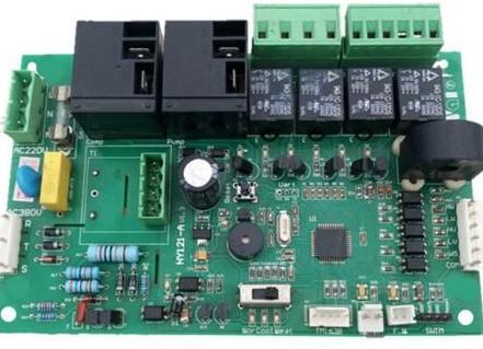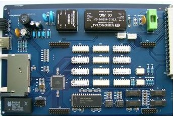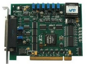
Pay attention to these requirements in PCB layout to avoid many unnecessary troubles.
1. Minimum space of SMD element LAYOUT. Ensuring a certain element spacing during SMD LAYOUT can reduce the probability of false welding, bridging, shadow effect and other problems during welding.
2. LAYOUT SMD components shall not be allowed within 3mm from the two panel edges of SMD PCB. This is mainly because the guide rail slot of the mounter requires that no component is allowed within 3~5mm of the PCB edge. 3mm is the minimum requirement. If this size cannot be guaranteed, V-groove or stamp hole can be used to lengthen the board, and the surplus board can be skimmed after welding.
3. SMD arrangement direction.

(a) The same PCB components shall be arranged in the same direction as far as possible.
(b) A test point with a diameter of 30mil must be left on the same gold track.
4. When SMD and PTH devices are mixed and wave soldering is used for one time,
(a) CHIP, SOT and SOIC elements shall be arranged perpendicular to the tin passing direction to avoid shadow effect.
(b) Elements whose height difference is too large shall not be arranged close to each other to avoid shadow effect.
(c) Any element should be arranged in parallel and perpendicular to the tin passing direction.
Shadow effect must be considered for PCB layout when wave soldering is used to solder SMD components. If reflow soldering is used, there will be no such problem. The so-called shadow effect, for example, when two SMD components with a large difference in component height are close together, if the high component passes the tin first, it is possible that the low body component that passes the tin later cannot eat the tin because of the resistance of the high body component. This is the shadow effect of the high body component.
(d) When the right angle (vertical) arrangement must be made, enough tin space must be reserved, and the space distance should be 0.635mm.
5. Solder dead corner caused by SMT LAYOUT (empty soldering)
The following figure shows the situations that may cause empty welding. In the specific LAYOUT, you need to consider whether the layout may cause empty welding during welding. In a word, you need to be flexible and not apply it mechanically.
6. V-CUT Reference Data
(1) FR-2, CME-1, OAK910 (semi glass fiber) PCB thickness 1.6mmV-CUT cutter depth 0.4mm × 2 sides.
FR-4 PCB thickness 1.6mm V-CUT cutter depth 0.5mm × 2 sides.
We always insist on delivering PCB products that are most suitable for technical requirements and most cost-effective to customers


