Over the past decade, commercial, industrial, Internet of Things, wireless connectivity, and a range of automotive radar applications have evolved to millimeter waves (24-100GHz). This rapid growth in millimeter-wave applications has created the need for multilayer printed circuit boards (PCBS) with millimeter-wave circuits. The transition to millimetre waves poses a number of challenges for the printed circuit industry, primarily conductor geometry and materials, as the shorter wavelengths reduce the feature size and amplify the relative tolerances inherent in PCB manufacturing.
Controlling production costs can be a complex engineering challenge. Costs must be built into the electrical design from the start, as the materials, substrate structure and PCB technology are determined here. Like all good engineering, the goal is to design a product that meets all performance requirements and has a high yield, taking into account all materials and manufacturing tolerances, resulting in a balance between cost and performance.
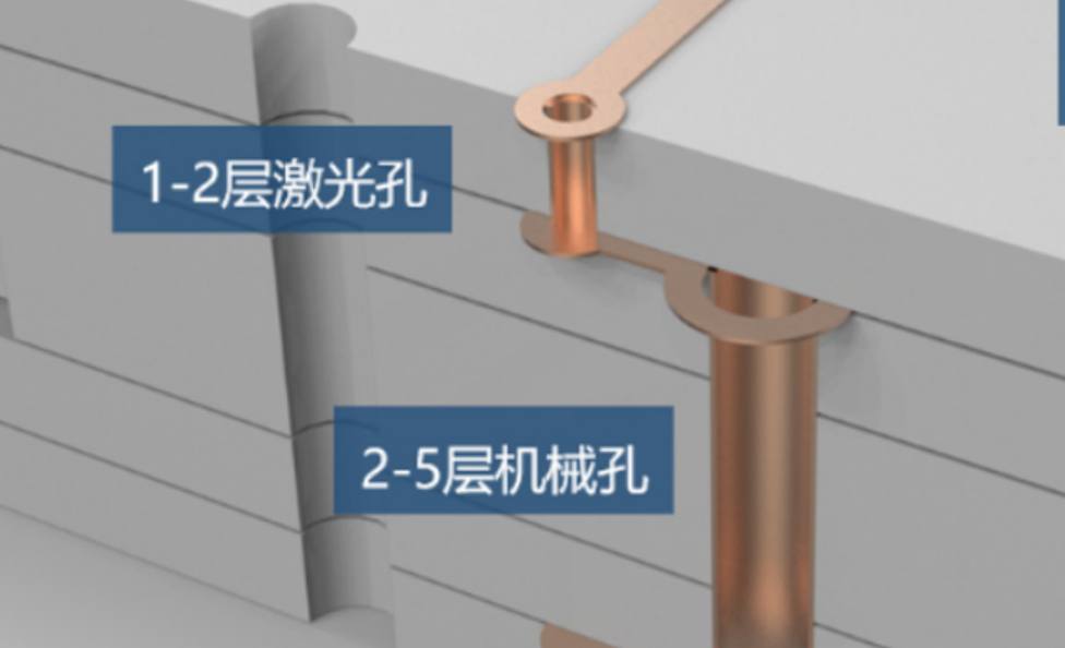
Finally, transmitting signals to different layers at millimeter-wave frequencies is a challenge. Regarding material properties and manufacturing difficulties, we present an example of forming various through-hole structures for millimeter-wave PCB applications. We introduce a surface-mounted cross assembly with simplified through-hole formation, which has several additional advantages: it facilitates rapid structural changes to conduct signals to different layers, addressing the impact on electrical properties. Millimeter-wave wavelengths are of the same order of magnitude as PCB geometry. Cost is another factor that adds complexity to the design, as many of the new millimeter-wave products are intended for consumer applications where the base material production ranges from tens of thousands to millions of pieces.
In its simplest form, printed circuits are manufactured using photo imaging and chemical etching processes. This is achieved by drilling circuit holes in copper foil laminates or multilayer laminates. After drilling, the panel is electroplated to form a copper layer, approximately 50 microns thick, on the drill hole and surface. Next, a photo resist is applied to the surface, which is imaged with ultraviolet light through the mask and developed to expose the unwanted copper. The exposed copper is chemically etched, leaving behind a finished circuit.
Etching into the dielectric also etches laterally into the sides of the conductor, making the process generally unsuitable for RF/microwave applications. Both the plated copper and the substrate must be etched to form a conductor, resulting in poor geometry and less than ideal conductor tolerances.
In order to overcome the problems of panel plating, most circuits are made using the "pattern plating process". Instead of electroplating the entire surface of the panel, a photo resist is applied to the base copper foil. The circuit pattern is then transferred to the resist coated panel using a light mask or direct laser imaging. After imaging and development, the exposed areas on the base copper foil will be electroplated to form a circuit pattern where the copper is also drilled.
To protect the circuit pattern and hole wall from the final etching, tin is plated on top of the circuit pattern. Next, the photo resist is stripped and the background copper foil is etched, followed by a tin strip, to produce a finished circuit. The pattern plating process offers better shapes and tighter tolerances than panel plating because only the underlying foil needs to be chemically etched, minimizing lateral etching that changes the side walls of the conductor. Installed with cross components, it has several additional advantages: it facilitates rapid structural changes, conducts signals to different layers, and addresses the impact on electrical properties.

The wavelength of the millimeter wave is of the same order of magnitude as the geometric size of the PCB. Cost is another factor that adds complexity to the design, as many of the new millimeter-wave products are intended for consumer applications where the base material production ranges from tens of thousands to millions of pieces.
In its simplest form, printed circuits are manufactured using photo imaging and chemical etching processes. This is achieved by drilling circuit holes in copper foil laminates or multilayer laminates. After drilling, the panel is electroplated to form a copper layer, approximately 50 microns thick, on the drill hole and surface. Next, a photo resist is applied to the surface, which is imaged with ultraviolet light through the mask and developed to expose the unwanted copper. The exposed copper is chemically etched, leaving behind a finished circuit. Etching into the dielectric also etches laterally into the sides of the conductor, making the process generally unsuitable for RF/microwave applications. Both the plated copper and the substrate must be etched to form a conductor, resulting in poor geometry and less than ideal conductor tolerances.
In order to overcome the problems of panel plating, most circuits are made using the "pattern plating process". Instead of electroplating the entire surface of the panel, a photo resist is applied to the base copper foil. The circuit pattern is then transferred to the resist coated panel using a light mask or direct laser imaging. After imaging and development, the exposed areas on the base copper foil will be electroplated to form a circuit pattern where the copper is also drilled. To protect the circuit pattern and hole wall from the final etching, tin is plated on top of the circuit pattern. Next, the photo resist is stripped and the background copper foil is etched, followed by a tin strip, to produce a finished circuit. The pattern plating process provides better geometry and tighter tolerances than panel plating because only the underlying foil needs to be chemically etched, minimizing the transversal that changes the side walls of the conductor.


