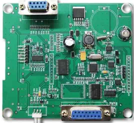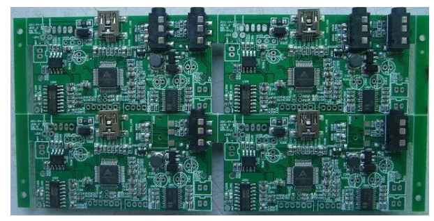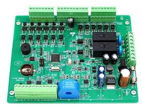
In the process of circuit board manufacturing, the circuit board welding and grounding work is a relatively important work. Even though we are in the circuit board in the other process of operation is relatively perfect. But because it does not take into account the grounding problem of the power supply, it may cause a series of adverse consequences. The following patch processing manufacturers to explain the circuit board design how to ground and how to analyze the circuit board schematic knowledge.
1. How to analyze the circuit board schematic diagram
For a professional engaged in PCB design, how to understand the schematic diagram of the circuit board is the most basic skills, only after understanding the schematic diagram of the circuit board can better understand the structure of the circuit board, circuit structure, wiring mode and so on. Here I give you a common circuit board analysis method:
1. Ac equivalent circuit analysis method: Using AC equivalent circuit board analysis method to analyze the circuit, it is necessary to draw the equivalent circuit diagram first. Thus you can analyze the AC situation in the circuit and its state. Simple can be understood as in the circuit board circuit input signal, circuit board in the circuit of each link on the current, voltage value will be in accordance with the law of the input signal changes.
2, frequency characteristics analysis method: the main principle of frequency characteristics analysis is to see whether the circuit board itself has frequency characteristics analysis, after the data analysis can be roughly calculated out of the circuit board in the center frequency, under the upper limit of the frequency and the basic situation of the band width.
3. Dc equivalent circuit analysis: DC equivalent circuit analysis is adopted. The first is that we need to draw the equivalent circuit diagram of the circuit AC. Then you can analyze the parameters of the DC system according to the circuit diagram. The analysis focuses on figuring out the transistor at static operating points and bias properties, interstage coupling mode, etc. Focus on the analysis of the relevant components in the circuit state and play a role.
4, time constant analysis: the use of time constant analysis method, the premise is a CRL diode PCB board. This method is mainly used to reflect the speed of energy accumulation and consumption of energy storage components. If the time constant is different, although its form and connection are similar, but the role is still different, common coupling circuit, differential circuit, integral circuit, decoupling circuit, peak detection circuit, etc. Finally, the actual circuit is compared with the basic principle, according to the role of the element in the circuit. As long as the above step by step analysis, you can clean and understand the circuit board schematic, of course, if you need to be more profound understanding, then you need to continue to learn to improve their relevant technical knowledge.

2. How to ground the circuit board design
Will directly lead to the performance of the circuit board deteriorates. Serious will also affect the circuit board qualified rate and other aspects of the problem. Therefore, we should attach great importance to the wiring of ground wire. To control the noise generated between the power supply and ground wire within a reasonable range, can not interfere with the operation of the circuit board. The cause of noise between ground and power lines is understood. The only thing we can do now is to suppress the noise in some way. The general way is to add a decoupling capacitor between the power supply and the ground wire to widen the width between the power supply and the ground wire as much as possible. The processing of the connecting leg in the large area conductor: in the ground of a large area, the legs of the components need to be connected with it, the processing of the connecting leg needs to be considered comprehensively. In terms of electrical performance, the welding pad of the component leg is fully connected with the copper surface, but there are some bad risks in the welding assembly of the components, such as: ① welding requires a high-power heater.
(2) easy to cause virtual solder joints. Therefore, taking into account the electrical performance and process needs, make a cross welding pad, called thermal isolation its main role is to make the possibility of virtual solder joint greatly reduced due to excessive heat dissipation of section during welding. The treatment of the ground leg of the multilayer plate is the same. Analog circuit and digital circuit co-ground processing method: At present, the circuit board on the market is no longer a single function circuit, now the main composition of the circuit board is a mixture of analog circuit and digital circuit, so in our wiring must take into account the impact of each other, especially on the ground noise interference, The relative frequency of digital circuit is relatively high. The relative sensitivity of analog circuit is relatively strong. The model line of high frequency must be far away from the sensitive analog circuit components as far as possible. And inside the board the digital ground and the analog ground are actually separate and they are not connected to each other, only at the interface (such as the plug) between the board and the outside world. There is a little bit of short-circuiting between digital and analog, but it is important to note that there is only one point of connection. There are also differences on the PCB, which is determined by the system design. Circuit board model line on the bottom wiring method: When the circuit board is made and wired, because there is not much left in the circuit board layer, some waste can not be avoided due to the factors of more layers, but also increase a certain amount of work, and the cost will be increased. In order to solve this problem perfectly, it is necessary to consider the wiring on the bottom layer. The first thing we need to think about is the power layer because we want to keep it intact.


