Recommendations for improving testability when using probe bed adapters
Latching hole
The configuration is diagonal
Positioning accuracy: ±0.05mm (±2mil)
Diameter accuracy is ±0.076/-0mm (+3/-0mil)
The positioning accuracy relative to the test point is ±0.05mm (±2mil).
The distance from the edge of the component should be at least 3mm
Do not penetrate contact
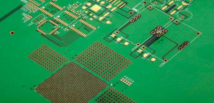
Test point
As square as possible
Test points should be 2.5mm apart if possible
Test point diameter at least 0.88mm (35mil)
Accuracy of test point size is ±0.076mm (±3mil)
Accuracy of spacing between test points is ±0.076mm (±3mil)
Tinned, end face can be welded directly
Be at least 3mm from the edge of the element
All test points should be possible on the back of the plug-in board
Test points should be evenly distributed on the plug-in board
At least one test point per node (100% channel)
Spare or unused gate circuits have test points
Multiple external test points of the power supply are distributed in different positions
Component mark
Sign text in the same direction
The type, version, series number and bar code are clearly identified
The component name should be clearly visible and labeled as close to the component as possible

2. Flash memory and other programmable components
Flash memory programming times can be very long (up to 1 minute for large memory or memory banks). Therefore, the reverse drive of other components is not allowed at this time, otherwise the flash memory may be damaged. To avoid this, all components connected to the control lines of the address bus must be placed in a high ohm state. Likewise, the data bus must be able to be placed in isolation to ensure that the flash memory is empty and can be programmed for the next step.
The in-system programmable component (ISP) has some requirements, such as Altera, XilinX, and Lattuce for their products, and other specific requirements. In addition to the mechanical and electrical preconditions for testability, the possibility of programming and corroborating data should be guaranteed. For Altera and Xilinx components, the Serial Vector Format SVF is used, which has recently become almost an industry standard. Many test systems can program such components and test signal generators with input data in the sequential vector format (SVF). These components are programmed by Boundary Scan-Kette JTAG, and sequential data formats are also programmed. When compiling programming data, it is important to consider the entire chain of components in a circuit and not to restore data to only the component to be programmed.
When programmed, the signal generator is automatically tested considering the entire component chain and other components are plugged into the bypass model. In contrast, the Lattice company requires data in JEDEC format and parallel programming through the usual input and output terminals. After programming, the data is also used to check the component function. The data provided by the development department should be as easy as possible to apply directly to the test system or through simple transformations.
3. What should we pay attention to for boundary scanning (JTAG)?
Components that consist of a fine grid based on complex components provide the test engineer with very few touchable test points. It is still possible to improve testability. Boundary scanning and integrated self-testing techniques can be used to shorten the test completion time and improve the test results.
For development engineers and test engineers, a testing strategy based on boundary-scanning and integrated self-testing technologies can certainly add to the cost. The development engineer must use the boundary scanning element (IEEE-1149.1- standard) in the circuit and try to make the corresponding specific test pins accessible (such as test data input -TDI, test data output -Tdo, test clock frequency -TCK and test mode selection -TMS and ggf). Test reset). The test engineer develops a boundary scan model (BSDL- Boundary Scan Description Language) for the component. At this point he must know what boundary scanning functions and instructions the component supports. The boundary scan test can diagnose short circuits and open circuits up to the lead level. In addition, automatic testing of components can be triggered by the boundary scan instruction "RunBIST" if specified by the developer. Especially when there are many ASICs and other complex components in the circuit, for which there is no conventional test model, the cost of developing a test model can be greatly reduced by boundary scanning components.
The amount of time and cost reduction is different for each component. For a circuit with IC, about 400,000 test vectors are needed if 100% detection is required, and by using boundary scanning, the number of test vectors can be reduced to hundreds at the same fault detection rate. Therefore, the boundary scanning method has special advantages when there is no test model or the nodes of the contact circuit are limited. Whether to use boundary scanning depends on the increased cost of development and manufacturing. Cost of border scanning must be balanced by time to fault detection, time to test, time to market, adapter cost and savings as much as possible. In many cases, salt industry solutions that combine traditional on-line testing methods with boundary scanning methods are the best solution.


