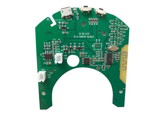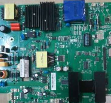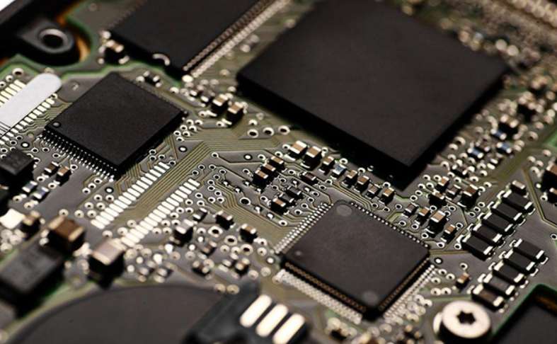
Shenzhen kingford is a circuit board design and production manufacturer that can provide circuit board design, circuit board proofing, and PCBA OEM. We have a professional circuit board design team, our own PCB board factory and SMT plant, and one-stop service for you to save worry and effort!
Circuit board design and production process
1. Prepare the means of production
The preparation of production materials is divided into two steps, including the PCB designer and the board factory's engineering audit personnel.
First of all, no matter the PCB design software is AD, Allegro or PADS, when the design is completed and the interactive production is about to take place, it is recommended to export the design document to Gerber for the sake of data confidentiality and actual production.
Gerber is currently the most common and versatile practice in the circuit board industry. One of the most common formats for Gerber data is RS-274-X. Simply put, it's the industry standard.
From the PCB designer's point of view, this is job done. The next thing is left to the factory.
After Gerber data is packaged and sent to the board factory, it will not be produced directly. After all, the board factory is also afraid of customer design on a bunch of problems, beyond their processing capacity. For example, the line spacing is too small, direct production is likely to short circuit. In case of short circuit between the power supply and GND, the whole circuit board sparks with lightning after power-on.
What do you do? Just dump the pot at the board factory.
Therefore, after the board factory gets the GERBER data from the customer, it also needs to review the production materials, which is also the reason why the production cost includes the engineering cost.
Plate factories usually use Genesis2000 to audit Gerber data. (Genesis2000 this software is mainly used by the board factory, if the engineer wants to check their own Gerber, learn a CAM350 is enough, there is no need to learn Genesis2000.)

The data review includes manufacturability check (line width, line spacing, solder resistance bridge, screen printing, etc.), electrical performance check (IPC network table comparison), and also adjusts the documents according to the customer's requirements, considering the factory's own situation (adjust line width or stacking according to impedance requirements, etc.).
CAM review is completed, the data is offline, and the preliminary preparation has been completed here.
2. Circuit board production and manufacturing
Circuit board manufacturing is a complex process, the whole process is roughly as follows:
More than 20 steps are summarized. In order to facilitate your understanding, we simplify the process and only list the key steps.
1. Cut the copper sheet into small pieces for production after drying;
2. Corrosion out of the inner line;
3. Press together so that the substrate and copper foil are combined together;
4. Drill holes, and then sink copper into the holes, so that the holes have electrical properties;
5. Make outer circuit;
6. Secondary copper to increase electrical conductivity;
7. Brush green oil (black oil, white oil, red oil, colorful oil);
8. Brush screen printing;
9. Surface treatment;
10. Molding (V-CUT, Routing, etc.);
11. Test (flying needle test, impedance test, metallographic section analysis, etc.);
So much for the streamlined process, but that's not to say the steps that aren't introduced aren't important. In the actual production process, every step has its necessity. In order to catch up with efficiency, some plate factories will compress some steps, such as reducing the time of high temperature baking or not baking at all, which will lead to some plates in the welding time of copper bubble cracking and so on.
3. Production and design
PCB production is in the factory, for many circuit design engineers contact opportunities are not much. However, a general understanding of PCB manufacturing and a reasonable estimate of the problems that may occur in the production process can make the design more reliable.
Here are a few small examples to illustrate:
1. Because the line is etched, there will be errors between the actual line width and the ideal value. Usually the line width below 10mil is ±1mil, and the line width above 10mi is ±10%. At the same time, the etching factor also affects the width of the upper and lower line. Therefore, in the calculation of impedance, the upper wire width of the outer layer is about 1mil smaller than the lower wire width, and the value of the inner layer is about 0.5mil.
2. Although the multilayer plate has rake holes for alignment, there are still errors when pressing, so the layer bias will be formed, and the layer bias can reach 3mil in some extreme cases. This may cause the two layers to overlap, or deviate from the reference plane.
3. There are two main production methods of screen printing, one is inkjet and the other is printed by making screen printing. For the latter, the position of the silk screen printing will have a large error. That's why you can't do accurate positioning through screen printing.
Each link of manufacturing may affect the performance of the circuit. There are too many contents involved here.
Why do you choose kingford for circuit board design and production?
1. Strength guarantee
▪SMT workshop: We have imported SMT machines and several sets of optical inspection equipment, with a daily output of 4 million. Each process is equipped with QC personnel, who can keep an eye on product quality.
▪DIP production line: We have two wave-soldering machines, among which there are more than 10 old employees who have worked for more than three years. The skilled workers can weld all kinds of plug-in materials.
2. Quality assurance, cost-effective
▪ High-end equipment can stick precision shaped parts, BGA, QFN, 0201 materials. Can also template patch, loose material hand.
▪ Sample and size batch can be produced, proofing from 800 yuan, batch 0.008 yuan/point, no start-up fee.
3. Rich experience in SMT and welding of electronic products, stable delivery
▪ Accumulated SMT SMT processing services for thousands of electronic enterprises, involving many kinds of automotive equipment and industrial control motherboard. The products are often exported to Europe and the United States, and the quality can be affirmed by new and old customers.
▪ On time delivery, normal 3-5 days after complete materials, small batch can also be expedited on the same day shipment.
4. Strong maintenance ability and perfect after-sales service
▪ Experienced maintenance engineers can repair all kinds of patch welding caused by bad products, to ensure the connection rate of each piece of circuit board.
▪ 24-hour customer service staff at any time response, the fastest speed to solve your order problems.


