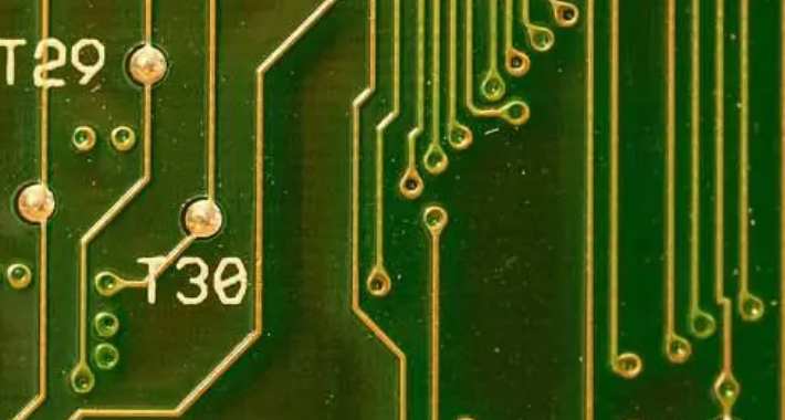
For light-emitting diodes, generally use long feet to represent the positive and negative terminals, long feet for positive, short feet for negative. Sometimes they cut a little bit off the side of the leds, and this can also be used to represent the negative electrode. On the circuit board is generally used screen printing "+" to indicate the positive terminal.
For ordinary diodes: the left side is negative, the right side is positive, that is to say, the use of silk screen or stained glass to indicate positive and negative polarity. Generally, the circuit board uses the following two ways to indicate positive and negative polarity.
Use screen printing on the circuit board to indicate the polarity of the diode. This is the comparison image. The other is to draw the schematic symbol of the diode directly on the screen printed circuit board.
The polarity representation of sticker LED is very confusing. Sometimes the representation between different package types within a manufacturer is all over the place. However, it is common to paint points or color strips on the cathode side of leds, and also to cut corners on the cathode side.
Common table sticker diode is also used on the body of the screen or stained glass to represent the negative terminal. In the image above, both diodes are negative on the left. In the circuit board diagram is generally: the left side is positive pad, the right side is negative pad.
1. Integrated circuit
For DIP and SO packaged integrated circuits with pins distributed on both sides, the top semi-circular notch is generally used to indicate that this direction is the top of the chip, and the first pin on the top left is the first pin of the chip. Also useful screen printing or laser on the top of a horizontal line to indicate. In addition, there are directly in the chip first foot next to the body with silk printing or directly in the injection molding press a pit. There are also some ics that cut a hypotenuse on the body of the starting edge of the first pin. The symbol of this type of IC on the circuit board is usually marked by a graphic with a notch on the top.
For QFP, PLCC and BGA of quadrilateral package, the integrated circuit of QFP package generally uses concave points, silkscreen dots, or determines the direction according to the model silkscreen on the body corresponding to the first pin. Some use the method of cutting off a corner to indicate the first foot, the counterclockwise direction for the first foot. It should be noted that sometimes 3 pits appear on a chip, so the corner without pits corresponds to the lower right of the chip. PLCC package because the body is relatively large, generally directly at the beginning of the first foot with pits to indicate. Some also do Angle cutting on the upper left side of the chip. In addition to the gold-plated copper foil at the lower left corner in the figure above, BGA packaging also uses the missing corner and concave points and silk screen dots to indicate the direction of the first foot.
2. Other devices
On the physical connector generally by positioning the gap to control the direction. There are also ones that write a 1 near the first foot or use a triangle for the first foot. Other devices generally draw a screen print on the circuit board that is consistent with the real thing to avoid inserting errors. For the through-hole installation of the exhaust resistance, generally on the circuit board with a silk screen to circle the common end, or write 1 near the first pin. In order to regulate the welding pad, screen printing, welding resistance and other requirements of the components on the circuit board, IPC has promulgated two related standards, namely, IPC-7351 and IPC-SM-840. However, in actual use, the device direction marking symbol made by the method of indicating the device direction defined by IPC is often blocked by the device body after welding, which is not suitable for inspection. The graphic design of the component pad should be adjusted according to the actual situation.

Summary: In a word, in the physical general discrete devices using long and short feet and screen printing or coloring method for polarity. For integrated circuits, the concave point, screen printing, notch, lack of Angle, lack of edge or direct indication of the way to mark the first foot. In the production of pad graphics, generally should be as far as possible according to the shape of the device drawing, while as much as possible to the device shape and positioning information reflected through the form of silk screen, in order to avoid artificial assembly, welding errors.
Shenzhen Prince Circuit Technology Co., Ltd. was established in 2007 in Daxing District, Beijing, and moved to Shenzhen in 2010. It is a high-tech enterprise dedicated to providing customers with one-stop high-end PCB manufacturing services from R&D samples to mass production. We deliver faster at the same cost and lower at the same delivery speed. Combined with market and customer demand, we also provide customers with CAD design, PCBA processing and components purchasing and other value-added services. The company is headquartered in Shenzhen, with PCB production and technology research and development base in Shenzhen. The CAD design company and PCBA processing factory are located in Changping, Beijing. It has set up service centers in many major electronic product design centers in China, and has provided rapid electronic manufacturing services to more than 3000 customers worldwide.
After years of grinding and precipitation, Prinplin Circuit has established a unique one-stop flexible manufacturing service platform, introduced a large number of senior talents in the industry, through long-term running-in experience has created a production and technical service team with outstanding composite ability. Our business covers CAD design, PCB manufacturing, PCBA processing and component supply.
Through in-depth resource integration, we provide customers with convenient one-stop purchasing experience, improve procurement efficiency, reduce supply chain management costs, and make the quality of complete sets of products more reliable. Products are widely used in industrial control, electric power, national defense, medical, automotive, security, computer and other fields. Fast delivery is our long-term commitment to practice, excellent quality is our solid foundation rooted in the electronic products market, lean manufacturing is our product online control process, professional service is our customers have been praised.
Shenzhen Princetron Circuit, as an innovative one-stop high-end electronic manufacturing services expert, will be committed to bring you more convenient experience, more intimate service and continuous innovation and progress!
Statement: The content and illustrations of this site are written by the author or reproduced on the website. The article and its accompanying pictures are for reference only. If there is any infringement or other problems, please contact the website to delete it in time.


