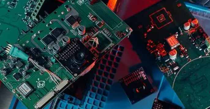
In the study of embedded development, we need to pay attention to the learning of practical knowledge, but the learning of basic knowledge must also learn step by step, only the foundation is solid, the content of the superstructure is easier to master, today and you share is the basic concept of embedded PCB design, let's take a look.
1. Concept of "Layer"
Similar to the concept of "layer" introduced in word processing or many other software to achieve the nesting and synthesis of graph, text, color, etc., Protel's "layer" is not virtual, but the actual copper foil layer of the printing board material itself. Today, electronic circuits are densely packed with components. Anti-interference and wiring and other special requirements, some new electronic products used in the printing board not only has the upper and lower two sides for wiring, in the middle of the board is also equipped with a special processing sandwich copper foil, for example, now the computer motherboard used in the printing board material more than 4 layers. Due to relatively difficult processing, these layers are mostly used to set the Power wiring layer with relatively simple wiring (such as Ground Dever and Power Dever in the software), and the large-area filling method is commonly used for wiring (such as ExternaI P1a11e and Fill) in the software. Where the upper and lower surface layers need to be connected to the intermediate layers, the so-called "Via" is used to communicate. With the above explanation, it is not difficult to understand the concept of "multi-layer pad" and "wiring layer setting". For a simple example, a lot of people finish wiring, to print out only to find a lot of wire terminal are not pad, in fact, this is to add their own device library.
Ignoring the concept of "Layer", did not define the characteristics of their own drawing and packaging pad as "Mulii layer". It is important to remind you that once you have selected the number of layers of the board to be used, you must close those unused layers so as not to cause trouble.
2. Through hole (Via)
To connect the line between each layer, drill a common hole at the junction of the wire that needs to be connected in each layer, which is the hole. In the process, a layer of metal is plated on the cylindrical surface of the hole wall by the method of chemical deposition to connect the copper foil in the middle of each layer, and the upper and lower sides of the hole are made into ordinary pad shape, which can be directly connected with the lines of the upper and lower sides, or not. In general, the design of the line on the hole treatment has the following principles:
(1) as little as possible
Once the hole is selected, it is necessary to deal with the gap between it and the surrounding entities, especially the gap between the middle layer and the line that is not connected to the hole, which is easy to be ignored. If it is automatic wiring, you can choose "on" item in the "Minimiz8tion" submenu to solve it automatically.
(2) The larger the required load capacity, the larger the required hole size, such as the power layer and the formation and other layers used to connect the hole is larger.

3. Silk Screen Overlay (Overlay)
In order to facilitate the installation and maintenance of the circuit, the required logo pattern and text code are printed on the upper and lower surfaces of the printing board, such as component label and nominal value, component outline shape and manufacturer's logo, production date and so on. Many beginners design the content of the screen printing layer, only pay attention to the text symbols placed neatly and beautiful, ignoring the actual PCB effect. They designed boards in which characters were either blocked by components or intruded into the soldering area to be brushed, or marked on adjacent components, all of which made assembly and maintenance very inconvenient. The correct silk screen layer character layout principle is: "no ambiguity, see stitches, beautiful and generous".
4. Specificity of SMD
Protel package library has a large number of SMD packages, namely surface welding devices. In addition to compact size, the most important feature of this kind of device is the single-sided distribution element pin hole. Therefore, the selection of this type of device to define the surface of the device, so as to avoid "Missing Plns". In addition, the text of this type of component can only be placed with the component on the surface.
5. Grid filling area (External Plane) and filling area (Fill)
As the name suggests, the network filler is a large area of copper foil treated into a network, and the filler is left intact. Beginner design process in the computer often can not see the difference between the two, in essence, as long as you magnify the surface at a glance. It is because it is not easy to see the difference between the two, so the use of more attention to the distinction between the two, to emphasize that the former in circuit characteristics has a strong inhibition of high-frequency interference, suitable for the need to do a large area of filling place, especially some areas as a shield area, segmentation area or large current power line is particularly suitable. The latter is mostly used in the general line end or turning area and other places that need to be filled with a small area.


