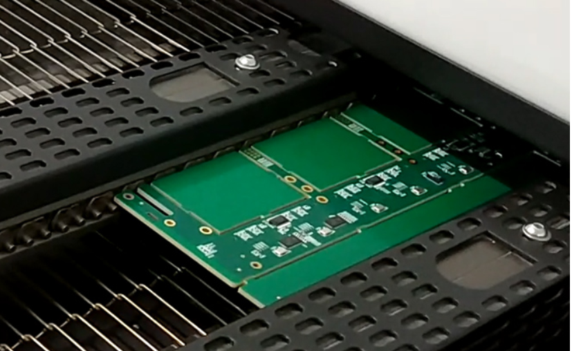
Integrate all data of flexible PCB (mechanical matching, design standards, circuit types and geometric structure interconnection forms), and make paper samples for matching and subsequent inspection at the same time:

1. Whether the terminal area is wide enough to meet the number and size requirements of the circuit;
Secondly, reasonable use and assembly machinery matching can be simply carried out, the number of lines can be calculated, multiplied by the line width and spacing, and then the minimum width of the flexible circuit board can be calculated according to the electrical requirements;
Third, the bottleneck of line width lies in the mechanical configuration, which determines the maximum number of lines in a single layer and also determines the number of layers in the overall design. At this point, there is a small problem: the resistance of the pcb is a function of the average width of the circuit. If the bottleneck area is short, the circuit can be reduced to compensate for conductivity by passing more lines in the single layer and increasing the width of other areas. In this way, it should be understood that when the multilayer flexible circuit board is bent to below a radius, the outer layer must be designed longer to compensate for the larger channel length. This part is called advanced stack design;
Circuit board
Fourth, all connections are kept on a flexible pcb circuit board;
5. The whole line harness is designed in a similar way (high current lines are designed in a high current mode, and sensitive lines are designed in a sensitive way).;
Sixth, review and optimize the overall pcb layout, pcb folding process, advanced design, hinge and tightness in use until a good shape is formed. Make copies and connect them in series to determine how many finished flexible circuit boards can be filled in the production board to estimate the cost. An effective design will have a high line density, so you can expect bottlenecks in the connector area layout. One idea is to estimate the number of flexible circuit boards at the early stage of development. These flexible circuit boards can have connection terminals on each layer, and then design the size of the pattern according to this number.
It is a headache for flexible circuit board design to keep the correct sequence of circuits and gradually become dense areas. In most cases, designers cannot configure pins or contacts very freely and flexibly. In the real world, flexible circuit board design can only be added later in the product plan. Most cases occur after the line connection configuration is determined, and it is almost impossible to rearrange. There will certainly be many situations at this time. The left line must reach the right plug or contact. PTH is a more general solution that allows the use of inter tier connections to reconfigure contact relationships. For designers who do not want to use PTH, the available solutions include external folding, reflective folding, pcb double-sided jumper combination and straight through connection.
From the design point of view, the design of a flexible circuit board is very special, but compared with the cell flexible circuit board, it also requires relatively high construction costs. Increased productivity is more effective, so implementation costs are lower. It should be reminded that if the technology and quality standards allow multiple contacts to be combined on one terminal, this design can break the complex circuit design, simplify it to a separable flexible circuit board, and use more popular terminals. Relatively small flexible pcb circuit boards can be configured into groups according to the type to facilitate testing, which can further reduce costs.


