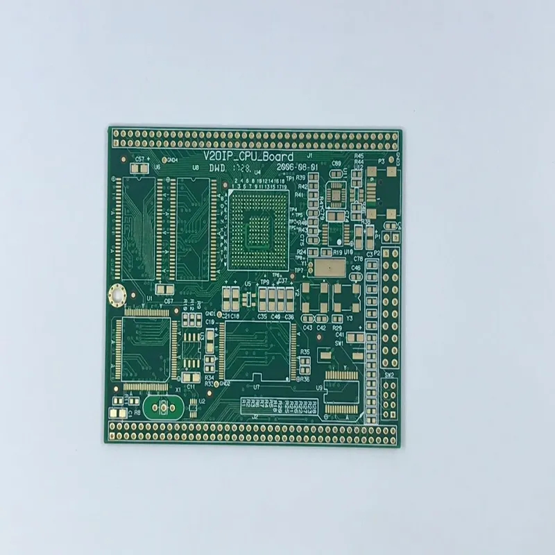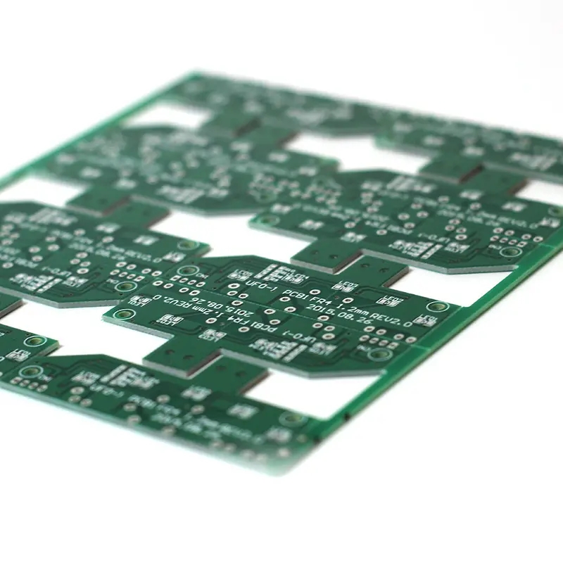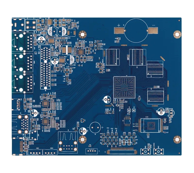
The factors that affect the exposure imaging quality of the circuit board factory
PCB manufacturers, PCB designers and PCBA manufacturers explain the factors that affect the exposure imaging quality of PCB manufacturers
If we want to make a small report on the process technology of the circuit board factory in the production process of the circuit board, it is possible to say that the last part is possible. Our operators strictly control every production detail of the circuit board factory. Today, we still share with us the factors that affect the exposure of the circuit board factory. We must take a look at what we are interested in.
The factors that affect the exposure imaging quality of the circuit board factory
Factors influencing the quality of exposure imaging in circuit board factory
(1) Selection of light source
In the circuit board factory (Shenzhen circuit board), any kind of dry film has its own unique spectral absorption curve, and any kind of light source also has its own emission spectral curve. If the main peak of spectral absorption of a certain dry film overlaps or mostly overlaps with the main peak of spectral emission of a certain light source, the two are well matched and the exposure effect is optimal. The spectral absorption curve of domestic dry film shows that the spectral absorption area is 310~440nm. Dysprosium lamp, high pressure mercury lamp and iodine gallium lamp have relatively high radiation intensity in the wavelength range of 310~440nnl, which is an ideal light source for dry film exposure.

(2) Control of exposure time
In the light editing process, the photopolymerization of the dry film does not complete the reaction at the sight of light, but requires a certain exposure time
Respond adequately:
When the exposure is insufficient, due to the incomplete polymerization of monomers, the film will become soft and the lines will not be clear during the development process,
The color is dim, even faint. During the pre-treatment or coating process, the film is warped, infiltrated, or even peeled off;
In the circuit board factory (Shenzhen circuit board), when the exposure is too high, it will cause problems such as difficult to develop, brittle adhesive film, and residual adhesive; Incorrect exposure will result in deviation of image line width. Excessive exposure will make the lines of graphic electroplating thinner and the lines of printed etching thicker. On the contrary, insufficient exposure will make the lines of graphic electroplating thicker and the lines of printed etching thinner. In order to determine the exposure time, it is generally recommended to use Rist 〇 n Grade 17 or sbuffer Grade 21 optical densitometer.
The factors that affect the exposure imaging quality of the circuit board factory
The circuit board factory (Shenzhen circuit board) also needs to pay attention to visual positioning during exposure positioning:
The visual positioning of circuit board factory is usually applicable to the use of diazo substrate, which is brown or orange translucent; But it is impervious to ultraviolet light. The bonding pad of the substrate is aligned with the hole of the printed board through the diazo image, and it can be exposed after being fixed with tape.
PCB manufacturers, PCB designers and PCBA manufacturers explain the factors that affect the exposure imaging quality of PCB manufacturers


