30 PCB circuit design and production terms, absolutely dry!
1. Annular Ring
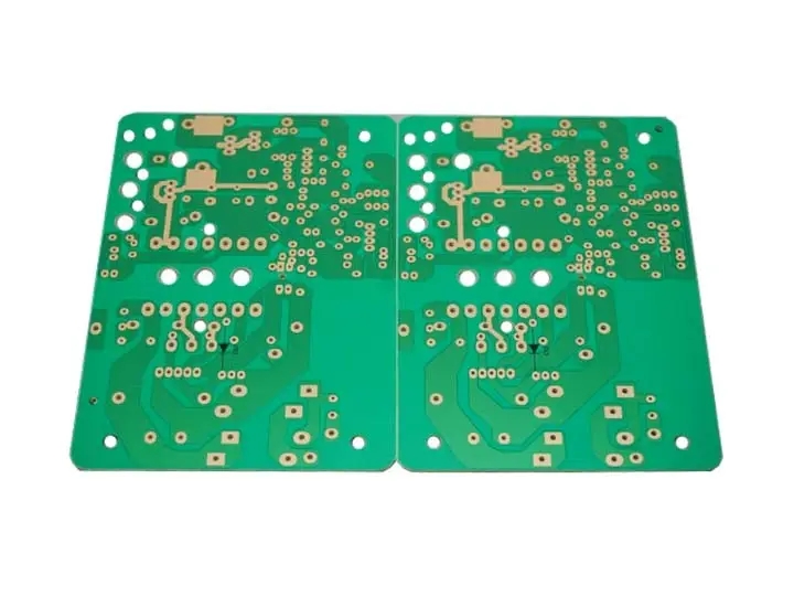
It refers to the copper ring wrapped around the wall of the connecting hole and pasted on the board surface. On the inner layer plate, this ring is often connected to the outside ground by a cross bridge, and is more often used as the end point or transit station of the line. In addition to being used as the transit of the line, the outer plate can also be used as the welding pad for the insertion welding of the part feet. It is also synonymous with Pad (ring) and Land (independent point).
2. Artwork negative
In the circuit board industry, this word often refers to black and white negatives. The brown "Diazo Film" is named after Phototool. The negatives used for PCB can be divided into "original negatives" Master Artwork and "working negatives" Working Artwork after re exposure.
3. Basic Grid
Refers to the vertical and horizontal grids where the conductor layout of a circuit board is located during design. The early grid spacing was 100 mils. At present, due to the prevalence of thin lines and dense lines, the basic grid spacing has been reduced to 50 mils.
4. Blind Via Hole
It refers to that in a complex multilayer board, part of the through holes are deliberately not completely drilled because only a few layers of interconnection are needed. If one of the holes is connected to the hole ring of the outer board, this special hole, such as a cup like blind alley, is called "Blind Hole".
5. Block Diagram
The assembly board and various required parts and components shall be framed in square or rectangular empty frames on the design drawing, and the relationship of each frame shall be connected one by one with various electrical symbols to form a systematic architecture diagram.
6. Bomb Sight bullet mark
Originally, it refers to the aiming screen of bombers. When PCB is making negative film, for the sake of alignment, such targets for upper and lower layer alignment are also set at each corner. The more accurate official name should be Photoshoppers' Target.
7. Break away panel
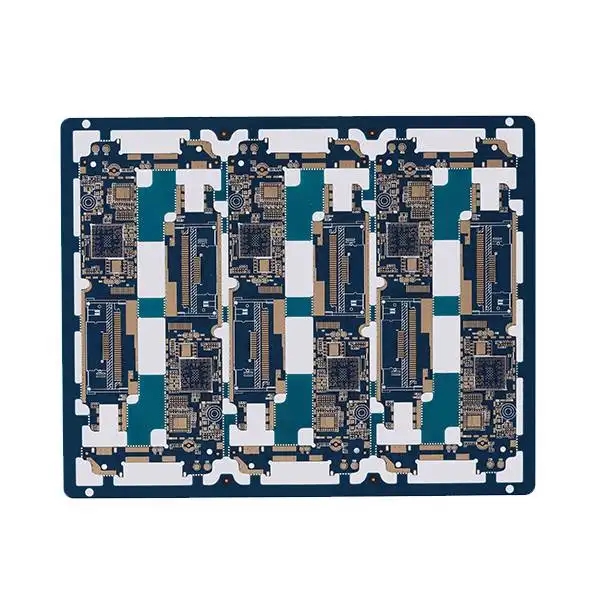
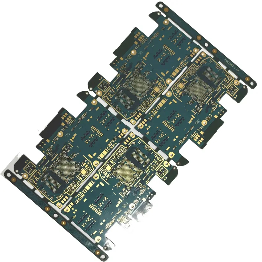
It refers to many small circuit boards. For the convenience of plug-in, placement, welding and other operations on the downstream assembly line, they are specially combined on a large board in the PCB manufacturing process for various processing. At the completion of the project, local cutting is conducted between independent small plates in the way of tool jumping, but several "Tie Bar" (Tie Bar or Break away Tab) with sufficient strength are reserved, and several small holes are drilled between the connecting plate and the plate edge; Or cut V-shaped notches at the top and bottom, so that the plates can be broken and separated after the assembly process is completed. There will be more and more small boards assembled together in the future, such as IC card.
8. Buried Via Hole
It refers to the local through hole of the multilayer board. When it is buried in the inner layers of the multilayer board, it becomes an "internal through hole" and is not "connected" with the outer plate, it is called an embedded guide hole or simply an embedded hole.
9. Bus Bar
It usually refers to the cathode or anode rod itself on the electroplating tank, or the cable connected to it. In addition, in the circuit board "in process", where the outer edge of the gold finger is close to the edge of the board, the original one is connected to a common wire (it must be covered during the gold plating operation), and then another one is connected to each finger with a small narrow piece (both to save gold, so its area should be reduced as far as possible). This kind of wire for conducting electricity is also called Bus Bar. The small piece connecting each individual finger with the Bus Bar is called Shooting Bar. When the board finishes cutting the shape, both will be cut off.
10. CAD Computer Aided Design
Computer Aided Design uses special software and hardware to digitally lay out circuit boards, and converts digital data into original negative films with an optical plotter. This kind of CAD is far more accurate and convenient than manual method for the pre production engineering of circuit boards.
11. Center to Center Spacing
Refers to the nominal distance between the center and the center of any two conductors on the board surface. If each conductor in a continuous arrangement has the same width and spacing (such as the arrangement of golden fingers), the "center to center spacing" is also called pitch.

12. Clearance
It refers to that on each inner layer of the multilayer board, if the conductor surface is not required to connect with the hole wall of the through hole, the copper foil around the through hole can be eroded to form a hollow ring, which is specially called "hollow ring". The distance between the green paint printed on the outer panel and each hole ring is also called Clearance. However, due to the increasing density of the current board circuit, the original leeway of this green paint is also being squeezed to almost nothing.
13. Component Hole
It refers to the through-hole for inserting the part foot on the finger board. The average hole diameter of this kind of foot hole is about 40 mil. Now, after the prevalence of SMT, the jack with large aperture has been gradually reduced, and only a few connector gold pin holes need to be inserted and welded, and most other SMD parts have been surface bonded.
14. Component Side
In the early days of circuit board full through hole insertion, parts must be installed on the front of the board, so it is also called "component face". The reverse side of the board is also called "Soldering Side" because it is only for the tin wave of wave soldering to pass through. At present, both sides of SMT boards need to be bonded with parts, so there is no "component face" or "solder face" anymore, but only the front or the back. The manufacturer name of the electronic machine is usually printed on the front, while the UL code and production date of the circuit board manufacturer can be added on the back of the board.
15. Conductor Spacing
It refers to the span of insulating substrate surface covered by a conductor on the circuit board from its edge to the edge of another nearest conductor, which is called conductor spacing, or commonly known as spacing. In addition, Conductor is a general term for various forms of metal conductors on circuit boards.
16. Contact Area
On the circuit board, it refers to the contact point between the golden finger and the connector. It is called the resistance when the current passes through. In order to reduce the generation of oxides on the metal surface, usually the positive gold finger part and the negative clamp of the connector should be plated with metal to suppress the occurrence of its "load resistance". The plug of other electrical appliances is squeezed into the socket, or there is contact resistance between the guide pin and its connector.
17. Corner Mark
On the negative of the circuit board, special marks are often left at the four corners as the actual boundary of the board. If the inner edge of these marks is connected, it is the boundary line of the contour periphery of the finished slab (Contour).
18. Counterboring
The circuit board can be locked and fixed in the machine with screws. For this matched non through hole (NPTH), the hole opening must be "reamed" to accommodate the nut, so that the whole screw can sink into the board surface to reduce the obstruction caused by the surface.
19. Crosshatching
For the sake of better adhesion between some large conductor areas on the circuit board surface and the board surface and the green paint, the sensing part of the copper surface is often turned off, leaving multiple crisscross cross lines, such as the structure of a tennis racket, which can resolve the floating crisis of large copper foil due to thermal expansion. The cross pattern obtained by etching is called Crosshatch, and this improvement is called Crosshatching.
20. Counterinking taper reaming, trumpet hole
It is another kind of screw hole for locking, which is mostly used in woodworking furniture, and rarely appears in the precision electronic industry.
21. Cross section area
The cross-sectional area of the circuit on the circuit board will directly affect its current carrying capacity, so it should be listed first in the design. The copper surface of the sensing part is often turned off, leaving multiple criss cross lines, like the structure of a tennis racket, so that the floating crisis caused by thermal expansion of a large area of copper foil can be resolved. The cross pattern obtained by etching is called Crosshatch, and this improvement is called Crosshatching.
22. Current Carrying Capacity
The conductor on the board can continuously pass the maximum current intensity (ampere) under specified conditions without causing deterioration of electrical and mechanical properties of the circuit board. The ampere number of the maximum current is the "current carrying capacity" of the circuit.
23 Datum Reference
In the process of PCB manufacturing and inspection, in order to correctly position the negative pattern on the board, a certain point, line, or hole surface is specially selected as the datum reference of its pattern, which is called Datum Point, Datum Line, or Datum Level (Plane), or Datum Hole.
24. Dummy Land dummy welding pad
In order to affect the height of the existing parts during assembly, the board surface under the belly of some parts needs to be padded to make the dispensing have better bonding force. Generally, the etching technology of the circuit board can be used to deliberately leave a "dummy copper pad" that is not connected to the pin but not connected to the power supply but only used for padding, which is called Dummy Land. However, sometimes due to poor design, there will be a large area of substrate surface without copper layer, with a few through holes or lines distributed. In order to avoid excessive current concentration of these independent conductors during copper plating, and for the sake of various defects, some nonfunctional dummy pads or wires can also be added to share some current during electroplating, so that the current density of a few independent conductors is not too high. These copper surfaces are also called Dummy Conductors.
25. Edge Spacing
It refers to the open space from the board edge to the "nearest conductor line". The purpose of this open space is to avoid the short circuit problem with other parts of the machine due to the conductor being too close to the board edge. The American UL safety certification pays special attention to this project. The white edge delamination and other defects of general plates cannot penetrate into half of the width of this "edge ground".
26. Edge Board contact
It is the outlet for the external connection of the whole board. Usually, two symmetrical sides of the board edge can be inserted into the matched board edge connector.
27. Fan Out Wiring/Fan in Wiring
It refers to the line and through hole and other conductors led from the welding pad around QFP, so that the welded parts can complete the interconnection with the circuit board. As the rectangular welding pads are arranged very closely, the external connection must use the open space inside or outside the rectangular square pad circle to route in a fan-shaped way, which is called "fan out" or "fan in". For thinner, shorter and denser PCBs, more welding pads can be placed on the outer layer to accept more parts, and the wiring required for interconnection can be hidden on the next layer. The connection between the welding pad and the lead wire between different layers is directly connected by the blind hole in the pad, and there is no need to do fan out fan in wiring. At present, many mobile phone boards of high-performance small wireless phones adopt this new stacking and wiring method.
28. Fiducial Mark optical target, reference signal
For the purpose of downstream assembly on the board surface to facilitate the operation of its visual aid system, a triangular "optical target" is added at the upper right and lower left of the space on the outer edge of each welding pad at the board surface assembly position by a large IC to assist the placement machine in optical positioning, as an example. In PCB manufacturing process, more than two reference marks are often added to align the negative with the board surface in the orientation.
29. Fillet
It refers to the arc filled at the vertical intersection of two planes or two straight lines. In the circuit board, it usually refers to the solder joint of the part pin, or the inner circle filling of the intersection of the T-shaped or L-shaped circuit on the board surface to enhance the mechanical strength and facilitate the current flow.
30. Film film
It refers to the film with circuit graphics. Generally, the thickness is 7mil and 4mil, and the photosensitive film includes silver halide in black and white, and azo compound in brown or other colors, which is also called Artwork.
PCB manufacturing, PCB design, PCBA processing manufacturers will explain 30 PCB circuit design and production terms for you, absolutely dry!


