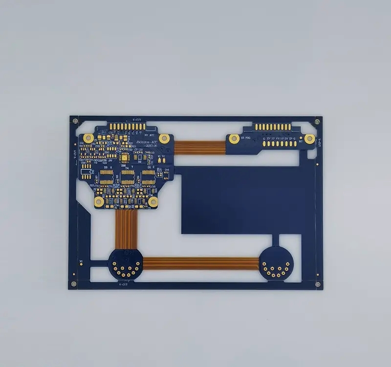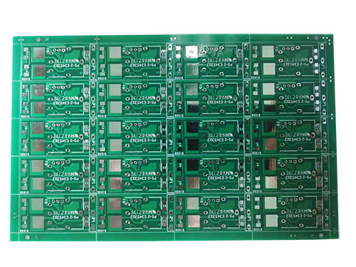
PCB board drilling quality, board temperature resistance test and board design risk
PCB manufacturers, PCB designers and PCBA manufacturers explain PCB drilling quality, board temperature resistance test and board design risks
When PCB drilling, there are always some defects, including drilling defects and in hole defects. The reliability of the metallization quality of these defects directly shadowed holes. What factors affect the drilling quality of PCB?
Printed circuit board is composed of resin, glass fiber cloth, copper foil and other materials with complex materials. There are many factors that affect the drilling process. A little carelessness in the processing process may directly affect the quality of the hole, and even cause scrapping in serious cases. Therefore, if any abnormality is found in the drilling overproduction, it is necessary to analyze the problem in time, propose corresponding process measures and correct them in time, so as to produce low-cost and high-quality printed boards.
2. The drilling quality is related to the structure and characteristics of the base material, the performance of the equipment, the working environment, the quality of the drill bit and the cutting process conditions. The specific conditions of these influencing factors can be analyzed to find out the exact influencing factors, so as to take targeted improvement measures.
3. Some of the factors that affect the drilling quality are mutually restrictive, and sometimes several factors work at the same time to affect the quality. For example, for the substrate with higher glass transition temperature (Tg) and the substrate with lower glass transition temperature, the drilling conditions are different due to the different brittleness of the substrate, and the feed speed for drilling the substrate with higher glass transition temperature is lower. Therefore, it is necessary to formulate correct drilling procedures and select appropriate drilling methods before drilling, and understand the structural characteristics, physical and chemical properties of the substrate very well.
How to conduct PCB board temperature resistance test?
In order to ensure the quality of PCB board, temperature resistance test is required. Generally, the maximum temperature resistance of PCB board is 300 degrees, 5-10 seconds; The temperature of lead-free wave soldering is about 260 ℃, and that of lead soldering is about 240 ℃. Then, how to do the PCB temperature resistance test?

1. Prepare PCB template and tin furnace.
Sample 5 pcs. of 10 * 10cm base plate (or laminated plate, finished plate) (no blistering and delamination of copper containing base material); Base plate: more than 10 cycles; Laminated plate: LOWCTE15010 cycle or above; HTg material: more than 10 cycles; Normal material: more than 5 cycles; Finished board: LOWCTE1505 cycle or above; HTg material has more than 5 cycles; Normal material has more than 3 cycles.
2. Set the temperature of the tin furnace to 288 ± 5 degrees, and use contact temperature measurement to calibrate.
3. First, soak flux with a soft bristle brush and smear it on the board surface; Then use the crucible pliers to take the test plate and immerse it in the tin furnace. Take it out after 10 seconds. Visually check whether there is any blistering or bursting plate. This is one 1cycle.
4. If the problem of blistering and bursting is found by visual inspection, immediately stop tinning to analyze the initiation point f/m; If there is no problem, continue to cycle until the board explodes, with 20 times as the end point;
5. The bubbling area needs to be sectioned for analysis to understand the source of the initiation point and take pictures.
In a word, the temperature resistance of PCB boards made of different materials needs to be understood in detail, and the maximum temperature should not be exceeded, so as to avoid scrapping of PCB boards.
How to reduce PCB design risk
In PCB design, if possible risks can be predicted and avoided in advance, the success rate of PCB design will be greatly improved. Next, let's talk about some experiences on reducing PCB design risks.
It is best to consider signal integrity issues at the system planning stage. Whether the signal can be correctly received from one PCB to another needs to be evaluated at an early stage, but it is not difficult to evaluate this problem. The knowledge of the whole signal integrity can be obtained through simple software operation.
2. In the process of PCB design, the simulation software is used to evaluate the specific wiring and observe whether the signal quality meets the requirements. The simulation process itself is very simple. The key is to understand the principle of signal integrity and use it for guidance.
3. Risk control must be carried out during PCB design. At present, many problems can not be solved by simulation software, which must be controlled manually by designers. The key to this step is to know where there are risks and how to avoid them. What is needed is signal integrity knowledge.
If the above three points can be grasped in the process of pcb board design, the risk of pcb board design will be greatly reduced, the probability of errors after the pcb board is punched will be much smaller, and debugging will be relatively easy. I wonder how much you know?
PCB manufacturers, PCB designers and PCBA processors will explain PCB drilling quality, board temperature resistance test and board design risks.


