What kind of circuit board processing is required for the sensor
Circuit board classification
Single panel
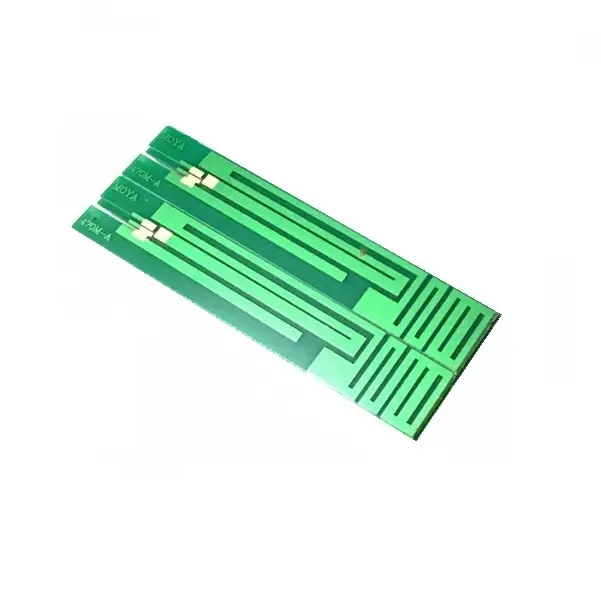
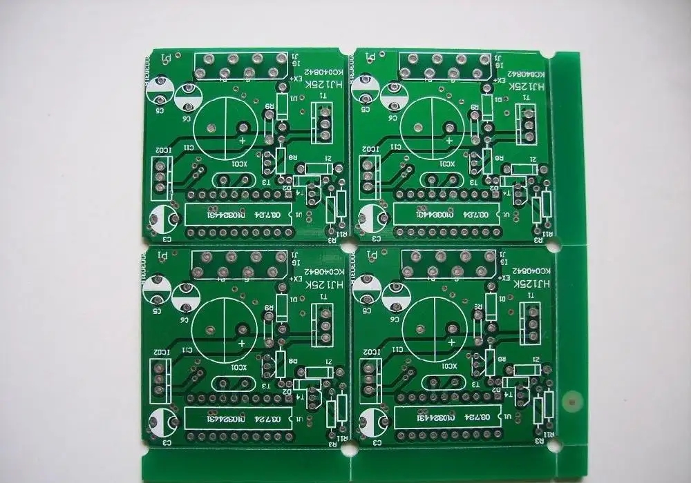
On the most basic PCB, parts are concentrated on one side and wires are concentrated on the other side. Because the wires only appear on one side, this kind of PCB is called single sided. Because there are many strict restrictions on the design circuit of a single panel (because there is only one side, and the wiring cannot cross and must go around a separate path), only early circuits use such boards.
Double-sided board
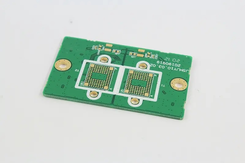
This kind of circuit board has wiring on both sides, but if you want to use wires on both sides, you must have proper circuit connections between them. This "bridge" between circuits is called a pilot hole (via). The pilot hole is a small hole filled with or coated with metal on the PCB, which can be connected with the wires on both sides. Because the area of the double-sided panel is twice as large as that of the single panel, the double panel solves the problem of staggered wiring in the single panel (it can be connected to the other side through the guide hole), and it is more suitable for circuits more complex than the single panel.

In order to increase the area that can be wired, more single or double sided wiring boards are used for multilayer boards. A printed circuit board with one double-sided as the inner layer, two single-sided as the outer layer, or two double-sided as the inner layer, and two single-sided as the outer layer, is a four layer or six layer printed circuit board, also known as a multilayer printed circuit board, when the positioning system and insulating bonding materials are alternately combined and the conductive patterns are interconnected according to the design requirements. The number of layers of the board does not mean that there are several independent wiring layers. In special cases, empty layers will be added to control the board thickness. Usually, the number of layers is even and includes the outermost two layers. Most motherboards are 4-8 layer structures, but technically, nearly 100 layers of PCBs can be achieved. Most large supercomputers use multilayer mainboards. However, since such computers can already be replaced by clusters of many ordinary computers, super multilayer boards have been gradually eliminated. Because all layers in the PCB are closely combined, it is not easy to see the actual number. However, if you carefully observe the motherboard, you can still see it.
Transducers, the English name of which is transducer, are detection devices that can sense the measured information and transform the sensed information into electrical signals or other required forms of information output according to certain rules to meet the requirements of information transmission, processing, storage, display, recording and control.
According to the manufacturing process:
Integrated sensors are manufactured using standard technology for the production of silicon based semiconductor integrated circuits. Usually, some circuits used for preliminary processing of the measured signal are also integrated on the same chip, such as the MEMS sensor which is now vigorously developed.
The thick film sensor is made by coating the slurry of corresponding materials on the ceramic substrate, which is usually made of Al2O3, and then conducting heat treatment to form the thick film.
Thin film sensors are formed by depositing thin films of corresponding sensitive materials on the dielectric substrate (substrate). When using the mixed process, some circuits can also be manufactured on this substrate.
Ceramic sensors are produced by standard ceramic process or some variant process (sol, gel, etc.). After the proper preparatory operations have been completed, the formed elements are sintered at high temperatures.
There are many common characteristics between thick film and ceramic sensor. In some aspects, thick film process can be considered as a variant of ceramic process.
The sensors are selected from the aspects of sensitivity, frequency response, linear range, stability and accuracy. The stability has a lot to do with the substrate material. The previous items mainly focus on the manufacturing process. In terms of stability, the most suitable non ceramic circuit board for the sensor is. The stability of ceramic materials is quite excellent. As long as the manufacturing technology can pass, ceramic circuit boards will undoubtedly be much easier to use than other PCBs.
The best manufacturing process of ceramic circuit boards now should be LAM technology. Laser Activation Metallization (LAM technology for short) uses high-energy laser beams to stabilize ceramics and metal ions, making them firmly combined.
However, at present, domestic sensor manufacturers are mainly small and medium-sized, and many of them are still using the film process, using the FR-4 substrate, which has a short service life and poor stability. When encountering a slightly worse environment, they directly went on strike. If you want to keep up with international standards, you still need to make great efforts.
The sensors still need ceramic circuit boards, which have been widely used in developed countries. At present, it is not technology that restricts the development of China. The upgrading of sensor circuit boards depends on the major manufacturers, who carry out technical innovation to become bigger and stronger, and China's sensor industry can catch up with the world PCB manufacturers, PCB designers and PCBA manufacturers will explain to you what kind of PCB processing is required for sensors.


