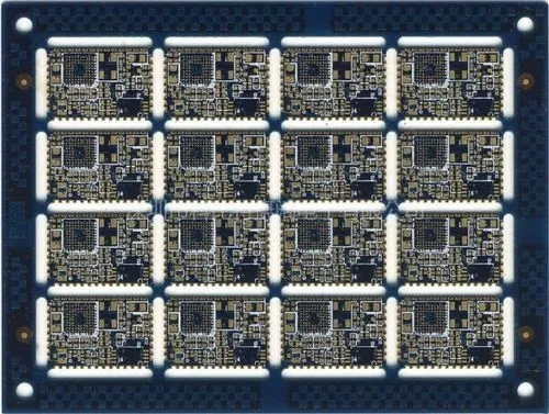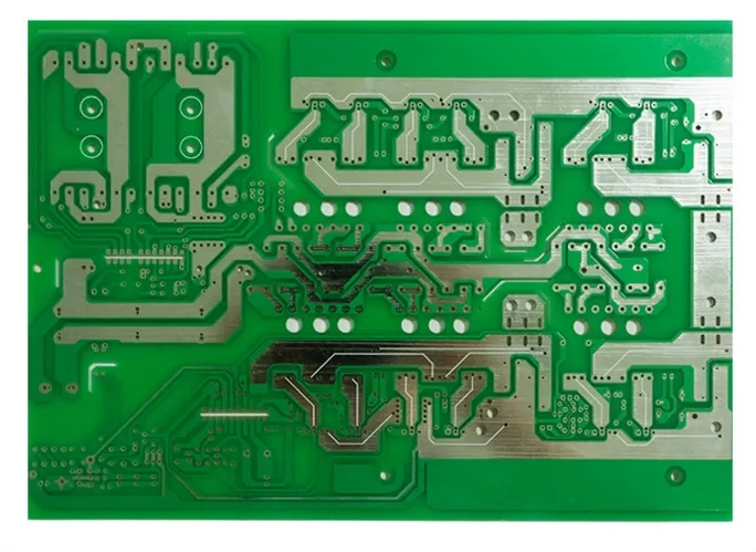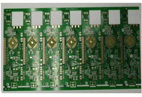
High frequency plate resistance welding bridge spacing and 5G characteristics
The circuit board manufacturer, circuit board designer and PCBA manufacturer will explain to you the problem of resistance welding bridge spacing of high-frequency pcb board and the main characteristics of the mobile terminal of high-frequency board in the 5G era
In view of the fact that the majority of small partners are very entangled in the problem of the gap between the resistance bridges of high-frequency PCB boards, I will write an article today to remove the confusion and entanglement in everyone's mind.
Solder mask (SM for short) of high frequency PCB. After the production of high frequency PCB, solder mask is usually printed. Because the color of commonly used ink for PCB is green, accounting for more than 90% of the PCB industry, solder mask is also called green oil. What are the functions of resistance welding? As follows: prevent the bridging short circuit of the line pad during welding, reduce the solder loss in the non welding area, provide a permanent electrical environment and chemical protection layer, and prevent the board from moisture and external damage.

Another point is that from an aesthetic point of view, high-frequency PCB boards can be dressed in gorgeous clothes to make them more beautiful.
Generally, in order to prevent short circuit between soldering and tin, we should ensure the solder bridge of the bonding pad. What is our conventional green oil resistance welding bridge. The bonding pad window is usually 2mil, so according to the above data, it can be calculated that the bonding pad spacing of our high-frequency pcb board design manuscript is 2mil+4mil (width of solder bridge)+2mil=8mil.
Main features of HF board in 5G era mobile terminal
With the continuous progress of science, there are three main characteristics of high-frequency boards used for mobile communication terminals in the 5G era:
High density: In the design of mobile terminals, high-frequency boards can create huge value for terminal customers every millimeter of space saved. By saving space, you can use larger, higher resolution displays, larger batteries, and more complex processors and components. All these can enhance the function of the device and enhance the overall user experience.
2. High heating: There are "impedance" and "dielectric loss" in the signal transmission of the high-frequency plate. With the high frequency or high-speed digitization of the signal and the increase of high power, the high-frequency plate continues to heat up. The first phase of 5g commercial frequency band in China is mainly below 6GHz, and it will reach 24-30ghz later. With the continuous improvement of 5g transmission rate, the amount of data transmission will greatly increase. In addition, the emergence of 3D video, cloud games, wireless charging and other applications will lead to a significant increase in the heating capacity of 5g communication terminals compared with the 4G era.
3. High frequency and high speed: With the arrival of 5g era, the obvious change of circuit board performance is high frequency and high speed. As 5g, Internet of Things and other applications will use higher frequencies, it will gradually increase from the past 3GHz to 6GHz or even 24-30gh22. Considering the high resonance frequency of 5g, it is necessary to control the impedance more strictly. If it is not formed in a very high precision form, the thin wire of 5G high-frequency board is likely to increase the risk of signal attenuation coefficient and reduce data integrity.
The circuit board manufacturer, circuit board designer and PCBA processor will explain to you the problem of resistance welding bridge spacing of high-frequency pcb boards and the main characteristics of high-frequency boards at mobile terminals in the 5G era.


