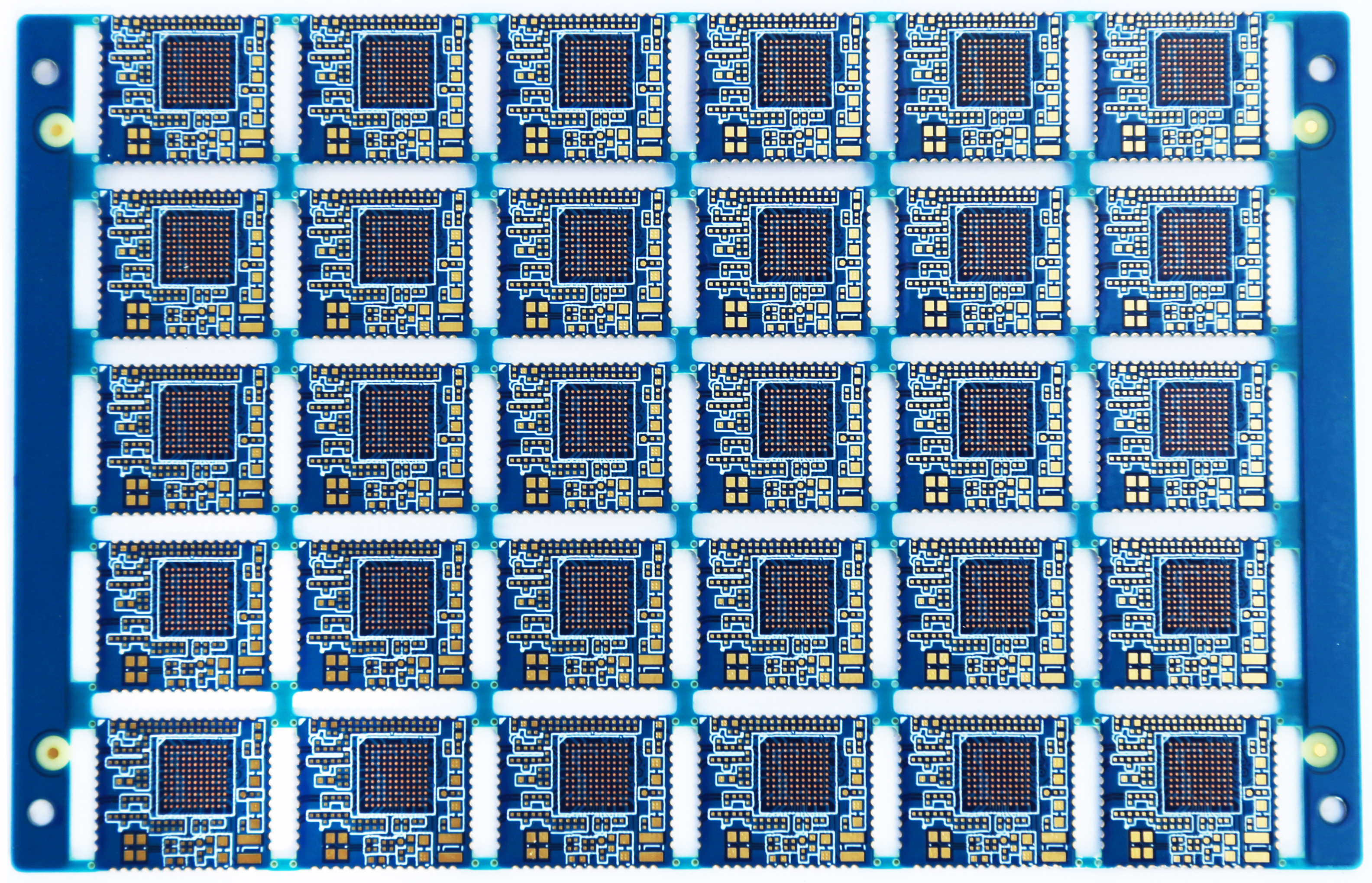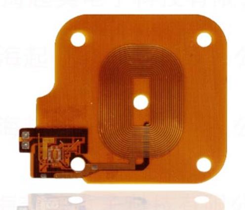
Power PCB layout and EMC of mobile phone wireless charging circuit board
What "unknown" secrets are revealed between the power PCB layout of mobile phone wireless charging circuit board and EMC's
Speaking of the difficulties of switching power supply, the mobile phone wireless charging circuit board manufacturer thinks that the PCB layout problem is not a great difficulty, but if a good PCB is to be laid, it must be one of the difficulties of switching power supply (poor PCB design may lead to the debugging and distribution of any debugging parameter, which is not alarmist). The reason is that there are still many factors to consider when PCB layout.
Such as: electrical performance, process route, safety requirements, EMC impact, etc; Among the factors considered, electrical is the most basic, but EMC is the most difficult to understand. The bottleneck of many projects is EMC; Now let's share PCB layout and EMC from 22 directions.
Sharing point 1: Only when you are familiar with the circuit, you can calmly carry out the EMI circuit of the mobile phone wireless charging circuit board factory's PCB design
The influence of the above circuits on EMC can be imagined. The filters at the input end are all here. The voltage sensitivity for lightning protection and the resistance R102 for preventing surge current (cooperate with the relay to reduce the loss). The key differential mode X capacitor and the Y capacitor that cooperate with the inductor for filtering, as well as the fuse that affects the safety gauge layout, each device here is crucial, and you should carefully taste the function and role of each device.

The EMC severity level should be considered when designing the circuit, such as the number of filtering levels, the number of Y capacitors and their positions. The selection of voltage sensitive size and quantity is closely related to our demand for EMC. Welcome to discuss the seemingly simple EMI circuit that actually contains profound truth for each component.
Sharing point 2: Circuit and EMC (the most familiar flyback main topology, see which key parts of the circuit contain the EMC mechanism)
The circuit in the figure above is circled: it is very important for EMC (note that the green part is not), for example, radiation. Everyone knows that electromagnetic field radiation is spatial, but the basic principle is the change of magnetic flux, which involves the effective sectional area of the magnetic field, that is, the corresponding loop in the circuit.
Current can produce magnetic field, which is stable and cannot be transformed into electric field. However, the changing current generates a changing magnetic field, which can generate an electric field (in fact, this is the famous Maxwell equation I use common language). The changing electric field can generate a magnetic field in the same way.
So we must pay attention to the places with switch status, which is one of the sources of EMC, and this is one of the sources of EMC (one of them here, of course, we will talk about other aspects later); For example, the dotted line loop in the circuit is the loop where the switch tube is turned on and off. Not only can the switching speed be adjusted during circuit design affect EMC, but also the area of the layout routing loop has an important impact!
Sharing point 3: The relationship between PCB design of mobile phone wireless charging board factory and EMC
1. The influence of PCB loop on EMC is very important. For example, if the flyback main power loop is too large, the radiation will be poor.
2. Filter wiring effect. The filter is used to filter out interference. However, if PCB wiring is not good, the filter may lose its due effect.
3. Poor grounding of the structure and radiator design will affect the grounding of the shielding plate.
4. The sensitive part is too close to the interference source, for example, the EMI circuit is too close to the switch tube, which will inevitably lead to poor EMC, and a clear isolation area is required.
5. Routing of RC absorption loop.
6. The grounding and wiring of Y capacitor and the position of Y capacitor are also critical!
Here is a small example:
As shown in the dotted line box in the figure above, the wiring of the X capacitor pin has been shrunk in. You can learn how to make the capacitor pin be wired externally (using squeeze current wiring). In this way, the filtering effect of X capacitor can reach the best state.
Sharing point 4: Preparations for PCB design: (Only when the preparation is sufficient, can the design be stable step by step and avoid design overturning and re starting)
In general, the following aspects will be considered during the design process. All the content has nothing to do with other tutorials, but is just a summary of your own experience.
1. The external structure size, including positioning hole, air duct flow direction, input and output sockets, needs to be matched with the customer's system, and also needs to communicate with the customer about assembly problems, height limits, etc.
2. Safety regulation certification, what kind of certification should be done for the product, where should the basic insulation creepage distance be enough, and where should the reinforced insulation be enough distance or grooved.
3. Packaging design: Is there any special period, such as customized parts packaging preparation.
4. Selection of process route: single panel double-sided board, or multi-layer board, shall be comprehensively evaluated according to schematic diagram, board size, cost, etc.
5. Other special requirements of customers.
The structure and process are relatively flexible. The safety regulations are still relatively fixed. What kind of certification and safety standards have been passed? Of course, there are some safety regulations that are universal in many standards, but there are also some special products, such as medical treatment, that are more stringent.
The following is a list of general products. The following are specific layout requirements summarized in IEC60065. Safety regulations should be kept in mind, and specific products should be targeted:
1. The distance between the input fuse pad parts and the safety specification is more than 3.0MM, and the actual layout is 3.5MM (in short, the creepage distance before the fuse is 3.5MM, and then 3.0MM).
2. The front and rear safety specifications of the rectifier bridge are 2.0MM, and the layout is 2.5MM.
3. The safety regulations after rectification generally do not require, but the distance between high and low voltage shall be reserved according to the actual voltage, and it is customary to reserve more than 2.0MM for 400V high voltage.
4. The initial interstage safety regulation requires 6.4MM (electrical clearance), and the creepage distance should be 7.6MM. (Note that this is related to the actual input voltage and needs to be calculated by looking up the table. The data provided is for reference only, subject to the actual situation)
5. For the first stage, cold ground and hot ground shall be clearly identified; 50. N identification, input AC INPUT identification, fuse warning identification, etc. shall be clearly marked; If you have questions about the above, you can also discuss and learn from each other!
Again, the actual safety distance is related to the actual input voltage and the working environment. It needs to look up the table for specific calculation. The data provided is for reference only, and the actual situation shall prevail.
Sharing point 5: Other factors should be considered in the safety regulation of PCB design
1. Know what kind of certification your products are and what kind of products they belong to, such as medical, communications, electricity, TV, etc., but there are many similarities.
2. In the safety regulations, understand the characteristics of insulation, which parts are basic insulation, and which parts are reinforced insulation. Different standard insulation distances are different. It is better to check the standards and calculate the electrical distance and creepage distance.
3. Pay attention to the safety devices of the product, such as the relationship between the magnetism of the transformer and the original and secondary sides;
4. The distance between the radiator and its surroundings is different. The insulation of the radiator varies with the ground connection. The ground connection is still cold, and the insulation of the hot ground is also the same.
5. Special attention shall be paid to the distance of insurance. The distance between the front and back of the fuse shall be consistent.
6. Y Capacitance and leakage current, contact current relationship.
PCB manufacturers, PCB designers and PCBA manufacturers will explain the power PCB layout and EMC of mobile wireless charging circuit boards.


