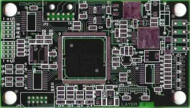
In fact, there are many ways to make plates quickly, such as the following:
1. Mechanical engraving
This method is the use of physical engraving method, the PCB board on the lead and pad and the unwanted copper coating separated. Of course, if you don't have such high professional equipment, you can also use a utility knife to carve yourself, for some very simple circuits or you can.
In special cases, the PCB copper layer can also be carved by high power laser, which is suitable for some special substrate circuit boards, such as ceramic substrate PCB, aluminum substrate PCB production, etc.
2. Chemical corrosion
The principle adopted by this kind of method is similar to the traditional PCB production process, which is to cover the welding pad and lead that need to be retained on the copper coating surface of PCB through exposure, thermal transfer printing, inkjet printing, oil pen painting and other methods, and then use chemical corrosion method to remove the remaining copper coating, so as to form the PCB that can be used.
Among them:
Exposure method: PCB board which needs special pre-coated photosensitive adhesive is exposed by ultraviolet lamp. After that, two steps of developing and etching are needed to obtain the circuit board.
Heat transfer printing method: Only need to print the PCB circuit diagram on the heat transfer paper through the laser printer, and then through the specific heat transfer machine to fix the toner on the PCB copper coating layer, after corrosion can obtain the required circuit board;
Inkjet printing: It is an inkjet printer that needs special modification to print the line directly on the PCB.
Oil pen drawing: the most simple, only need to use an ordinary oil-based marker pen, coupled with the ingenious drawing, you can.
In addition, to draw the circuit diagram, you can also use the stepper motor to drive the pen to complete the circuit drawing on the circuit board.
3. Paste the circuit
For some simple leads, through the current is relatively large circuit, can be pasted by copper foil tape.
4. Conductive ink
This is done by adding a few silver nanoparticles to the ink, allowing it to quickly dry and conduct electricity, forming a conductive metal film. On this basis, the required circuit can be formed.

The circuit formed in this way has the advantage that it can form the required circuit on any object surface, but the width of the line is relatively large, and the resistance of the line is larger, suitable for some simple control signal circuit production.
5. Castles in the air
To achieve the highest state of the circuit, that is no circuit board circuit. In fact, in early circuits, because the electronic components were so large, the circuit was welded directly between the pins of the components using leads. Today's device ratios are small, and in special cases, removing the circuit board can greatly reduce the size of the circuit.
Heat transfer printing
1, heat transfer printing method it is not only very fast to make, basically can be completed in one minute circuit board production, and the required materials are very cheap.
Laser printer;
Heat transfer paper;
Heat transfer machine;
Corrosive liquid: hydrochloric acid and hydrogen peroxide;
Single-side copper-clad plate;
Among them, the price of the heat transfer machine is also very cheap, only a few hundred dollars. As for the other consumables, they are readily available.
2, quick plate in the little secret
In order to save time and obtain high-precision circuit boards, there is a little secret, which is probably most people who make PCB tend to ignore, that is to use PCB coated with thin copper layer for the manufacture of circuit boards.
In circuit board slimming - The effect of PCB in thermal transfer plate after using copper reduction the effect of PCB with different copper thickness was compared. It can be seen that the thin PCB after copper reduction can realize the circuit production of 4mil line width. This has reached the standard of ordinary PCB production process.
Of course, in order to achieve the dual panel effect, the flexible use of 0 ohm resistance is a combination of experience and inspiration.


