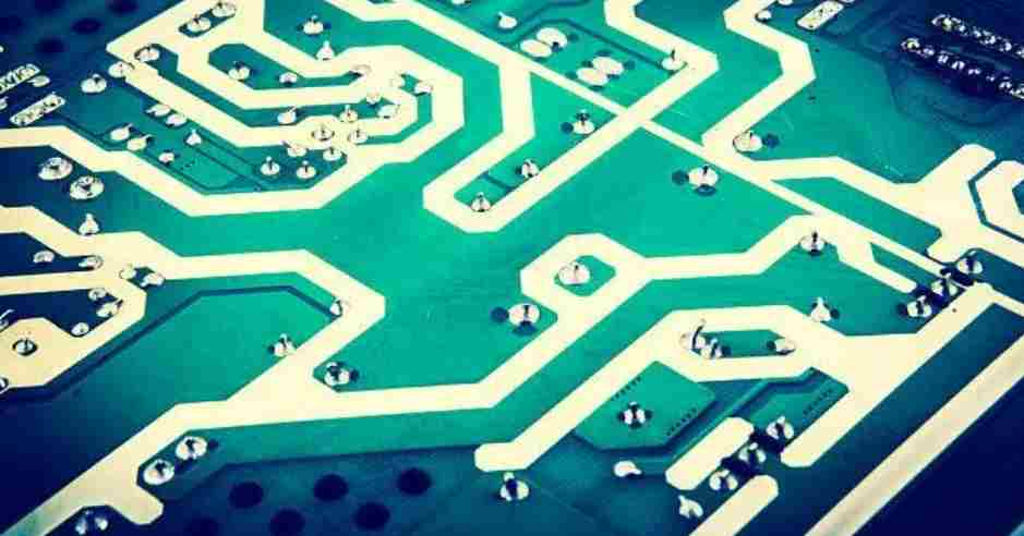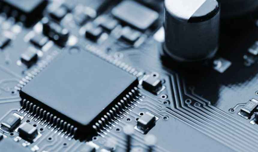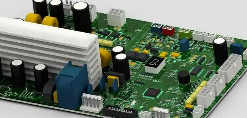
PCB pure water equipment and circuit board pure water equipment mainly refers to the water purification equipment when some processes need to be cleaned in the production process of PCB and circuit board. The water quality requirements are generally 10us, if there are higher requirements, the water quality is generally less than 1us. Circuit board pure water equipment generally uses reverse osmosis pure water equipment. If the water quality is pure water with electrical conductivity below 10us, it is also necessary to configure mixed bed or EDI equipment to meet the water requirements. The following processes of PCB circuit board production need pure water cleaning: copper plating, gold plating, silver plating, nickel plating, tin plating. Can be used for multilayer circuit board, double layer circuit board and single layer circuit board production.

According to different water quality requirements, it is mainly divided into two technological processes:
Pure water equipment less than 10us:
Original water tank - stainless steel booster pump - multi-media filter - activated carbon filter - precision filter - reverse osmosis host - pure water tank - water point
PCB circuit board ultra-pure water process:
Original water tank - stainless steel booster pump - multi-media filter - activated carbon filter - precision filter - reverse osmosis host - ion exchange mixing bed - UV sterilizer - polishing mixing bed - interrupt filtration - water point
Features and advantages of PCB pure water equipment for circuit board washing
1. Two-stage RO+EDI water treatment process is mature, reliable, advanced and highly automated.
2, the treatment of ultrapure water quality meets the requirements, high water utilization rate, reliable operation, economic and reasonable.
3, PLC+ touch screen control, a full set of high degree of automation, high system stability, saving labor and maintenance costs.
PCB cost driver: Simplify to reduce board cost
PCB costs are not based solely on complexity
The most important point is that the cost of a board depends on more than its overall complexity. In many cases, a single process, tolerance, or function can turn an otherwise inconspicuous board into a low-yield board, which may be encountered when you distribute it to potential manufacturers to resolve deviations or prohibit bidding altogether. Offer.
Low end technology PCB design
At the lower end of the technology spectrum, mechanical labeling is a source of concern. For example, we occasionally see double-sided PCBS where the required material thickness is often not available or has unrealistic thickness tolerances.
Our first strategy is always to suggest a standard thickness that is easy to procure and inexpensive. This simple suggestion can solve the problem effortlessly 75% of the time, many of which are due to PCB designers' unfamiliarity with the standard. In other cases, however, the board may be an afterthought in a larger project, designed to fit inside a case with some space inside. If it is a multilayer printed circuit board, then the manufacturer can usually mix and match the core and prepreg sheets to laminate to the correct total thickness.
However, if you work with 2 layers, the cost will increase. Because the manufacturer is not a core material manufacturer listed by UL, this also prevents the PCB manufacturer from certifying that the resulting material is UL compliant. Therefore, it is best to design a standard material thickness with a standard tolerance.
Intermediate technology PCB design
In mid-level design, a single micro BGA (or similar high density device) may increase your cost. Even if the rest of the PCB follows very standard design rules, the manufacturer must adapt the process to accommodate a high-end function. It essentially becomes the "worst case" element of the design, thus introducing the need for special treatments and/or special materials.
While the added cost may not be as high as a design that includes many difficult features, the price will still be significantly higher than the standard price. Sometimes minimal functionality is absolutely necessary, it is absolutely necessary to function properly or to reduce the PCB size to fit the available space. In this case, the extra cost is worth it. Still, before choosing the smallest available processor, it's worth at least considering other components with more forgiving features.
Advanced technology PCB design
Many new PCB designs absolutely require high-end materials and processing, so it is impossible to produce them cheaply. High frequency laminates, multi-period high density interconnect (HDI) cycles with sequential lamination and features such as cavity formation and backdrilling all contribute to the high cost of truly complex designs. Embedded components and laser direct imaging (LDI) are two technologies that can be used to design smaller and smaller PCBS.
In the quest for smaller and smaller miniaturization, some passive components have long been used as through-hole types, but are now moving toward inner layers that are passed through slave sheets before scaling down to smaller and smaller surface-mount versions. Embedded components require special materials that can be laminated between the other layers of the board, thus increasing functionality while eliminating clutter on top and bottom surfaces. As appealing as it sounds, not every manufacturer offers embedded component processing, and those manufacturers will charge a premium price. As with any other high-end design feature, it's useful to know that this technology exists. It is also important not to design increased costs unless they are lower in other ways.
Direct laser imaging has become increasingly common for extremely narrow HDI boards whose routing/space requirements are beyond what can be reproduced by conventional film processing. The main advantage of LDI is that it can produce smaller, tighter and more consistent feature sizes than traditional film to film exposures. Aside from the investment in equipment, the downside is that each panel takes more time than exposure. Exposure takes a few seconds, while LDI requires the laser to move around the design, forming feature after feature, in the same way as a CNC milling machine or a flying probe continuity tester. Throughput has improved considerably since LDI was first introduced, but it is still an advanced process, provided at a premium price. If you can lay out the PCB with more lenient design rules, LDI is not necessary.
Summary
The key point is the same for all elements of your PCB design: try to exhaust the possibilities of existing low-cost technology before moving on to more advanced features. As mentioned earlier, some applications require a state-of-the-art approach to meet design requirements, and the necessary equipment and processes do exist to make this design a reality. Still, it's worth examining every element of your design to make sure you really need more complex features that might add to the cost and eliminate unnecessary features. The benefits of eliminating unnecessary complexity are lower costs and more predictable manufacturing.


