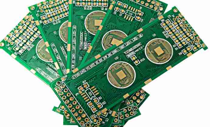
LED lamps and lanterns are used in many families because of their advantages of energy saving, environmental protection, safety and power saving. However, due to the high price of LED lamps, it is still difficult to achieve popularity. Many manufacturers are using ceramic COBs to process LED, because this can further reduce the cost of LED energy-saving lamps.
However, the whole LED market is in the situation of electricity shortage, money shortage, manpower shortage, high cost, low profit, so that the entire operating cost rises, so that the gross profit level of LED packaging enterprises declines. Using COB packaging, thus reducing costs.

From the point of view of packaging, because LED is generally divided into discrete and integrated two forms of packaging. The COB ceramic circuit board is mainly a form of personalized packaging, so that COB can directly put a number of chips directly packaged on the circuit board, so as to strengthen the cooling system, so as to reduce the cost of the support process.
In fact, COB, as the mainstream trend of future lamps, can not only package chips through ceramic COB, but also realize the reasonable configuration of LED chips, so that the heat can be more easily transmitted to the lamp shell.
Keyou Circuit is a company committed to PCB rapid proofing and mass production, with high precision single side/double side/multilayer circuit board (1-26 layers), thermoelectric separation copper substrate,COB ceramic substrate, multilayer industrial circuit board, power pcb board, medical circuit board, security PCB board, communication PCB board, automotive circuit board, instrument circuit board, military circuit board, complex Joint mother bar copper substrate, foldable metal substrate,FPC soft and hard combined board, quality assurance, delivery on time, to sales as one of the high-tech enterprises.
Precautions for the use of COB ceramic substrate
COB packaging can improve light efficiency and reduce cost, LED lamp manufacturers are more and more using COB ceramic substrate packaging. Precautions for the use of COB ceramic substrate are as follows:
Take and place: do not touch the ceramic directly with your hands. It will turn yellow after heating after contamination.
Storage: If it cannot be used in time after opening, put it in the drying cabinet and avoid high humidity. Pay attention to whether the sealing ring of the drying cabinet contains sulfur, which is easy to vulcanize with ceramics. If the external electrode needs to be preserved for a long time, the coating method can be used to avoid the yellowing of the electrode.
Chip: The chip shall be a medium power chip with high optical efficiency (≤0.5W). The layout of the chip shall not be too dense, and the spacing shall be greater than twice the thickness of the chip.
Solidification: The solidification of the ceramic can be pressed by the steel plate.
Welding wire: welding wire temperature is higher than the ordinary temperature, welding wire process parameters need to be carefully inquired about the corresponding manufacturers, different manufacturers of temperature will be different.
Jig: jig can not be used similar to the use of aluminum substrate jig, because the ceramic is hard, and aluminum substrate toughness, jig platen requirements parallel up and down, and the pressure can not be too high, the pressure can not move, in and out of the material need to clip tray, not directly clip the ceramic.
Dry: Dry and dehydrate before use.
Electrode welding: when the light source is connected to the welding electrode, the solder can be melted. It is not allowed to heat the electrode for a long time, because the solder will impinge on silver, resulting in silver separation and damage the light source.
Heat conduction grease: The heat conduction grease on the back of the light source should not be too thick. After coating, scrape flat with a plastic sheet, and the radiator surface is the same. Because the thermal conductivity of thermal grease is worse than that of ceramic, too much heat can not be transferred well.
Alumina ceramic base and aluminum nitride ceramic circuit board, using Laser Activation Metallization technology (LAM technology), high bonding strength between the metal layer and ceramic, good electrical conductivity, can be welded many times, the thickness of the metal layer is adjustable in 1μm-1mm, The maximum L/S resolution can reach 10μm, which can be easily and directly realized through hole connection.
Comparison of metal sinking process and other processes of PCB circuit board
1. Comparison of welding strength:
Sunk gold circuit board after three high temperature full solder joint, bright
OSP plate after three high temperature solder joints for gray color, similar to the color of oxidation
After three high temperature welding can be seen that the gold plate solder joint full bright welding good and will not affect the solder paste and flux activity, and OSP process of the solder joint gray no luster, affecting the solder paste and flux activity, easy to cause air welding, repair increase
2. Comparison of heat dissipation:
The thermal conductivity of gold is good, and the welding pad made of it has the best heat dissipation because of its good thermal conductivity. Good heat dissipation PCB board temperature is low, chip work more stable. The gold plate has good heat dissipation, and can use comprehensive heat dissipation holes in the CPU bearing area and BGA-type component welding base on the Notebook board, while the OSP and silver plate have average heat dissipation.


