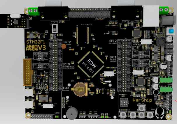
Single chip emulator is a set of hardware device specially designed and manufactured for the purpose of debugging single chip software.
SCM is the same as PC in the architecture, also includes * processor, input/output interface, memory and other basic units, so the software structure of PC and other devices is similar. Therefore, microcontroller in the process of software development also need to debug the software, observe the results, eliminate the problems in the software. However, due to the application of the microcontroller problem, it does not have a standard input and output device, limited by storage space, it is difficult to accommodate the software used for debugging procedures, so to debug the microcontroller software, the use of microcontroller simulator. Single chip emulator has the basic input and output device, with the support of program debugging software, so that the single chip developer can input and modify the program through the single chip emulator, observe the results of the operation of the program and the intermediate value, at the same time with the single chip supporting hardware detection and observation, can greatly improve the efficiency and effect of single chip programming.
The early single-chip emulator was a set of vertical devices with a key board and a display for inputting programs and displaying running results; With the popularity of the PC, most of the new generation of emulators are using the PC as the standard input and output device, and the simulator itself becomes the interface between the computer and the target system, the simulation way also from the beginning of the machine code development to assembly language, C language simulation, simulation environment and the PC language programming and debugging environment is very similar.
The simulator generally has a simulation head, used to replace the target system in the single chip microcomputer, that is, use the plug to imitate the single chip microcomputer, which is the name of the single chip emulator.

At present, with the microcontroller miniaturization, chip and the wide application of the microcontroller with ISP, IAP and other functions, the application range of the traditional microcontroller simulator has been reduced. And software SCM simulator (that is, SCM simulation program) is widely used, SCM simulation program is running on the personal computer, can simulate the hardware environment of SCM operation to a certain extent, and in the environment to run SCM target program, and can debug the target program, breakpoint, variable observation and other operations, It can greatly improve the debugging efficiency of SCM system. Pure software single-chip emulator is often integrated with the hardware design program released together, so that ** can develop the single-chip hardware and software synchronously.
In PCB circuit board design, the anti-ESD design of PCB circuit board can be realized through layering, proper layout and installation. In the design process, most of the design can be modified to add or subtract components through prediction. The PCB layout and wiring can be adjusted to prevent ESD
Static electricity from the human body, the environment and even inside electronic equipment can cause various damage to the precision semiconductor chip, such as penetrating the thin insulation layer inside the component; Damaged grids of MOSFET and CMOS components; Trigger locking in CMOS devices; PN junction with short circuit reverse bias; PN junction with short circuit forward bias; Melt the welded wire or aluminum wire inside the active device. In order to eliminate electrostatic discharge (ESD) interference and damage to electronic equipment, it is necessary to take a variety of technical measures to prevent.
In the design of PCB circuit board, the anti-ESD design of PCB circuit board can be realized through layering, proper layout and installation. In the design process, most of the design can be modified to add or subtract components through prediction. The PCB layout and wiring can be adjusted to prevent ESD. Here are some common precautions.
Multilayer PCBS are used whenever possible. The ground plane and power plane, as well as the closely spaced signal wire-ground spacing, reduce common-mode impedance and inductive coupling to 1/10 to 1/100 of that of a double-sided PCB compared to a double-sided PCB. Try to place each signal layer next to a power layer or ground layer. For high density PCB boards with components on both the layer and the bottom surface, with very short wiring and many padding places, consider using inner wiring.
For double-sided PCBS, a tightly interwoven power supply and grid are used. The power cord is next to the ground wire, between the vertical and horizontal lines or filling areas, and should be connected as much as possible. One side of the grid should be less than or equal to 60mm and, if possible, less than 13mm.
Make sure each circuit is as compact as possible.
Put all connectors aside if possible.
If possible, steer the power cord away from the lead-in of the card and away from areas prone to direct ESD impact.
On all PCB layers below the connectors leading out of the case (which are susceptible to direct ESD damage), place wide case floors or polygonal filler floors and connect them together with holes at approximately 13mm intervals.
A mounting hole is placed on the edge of the card, around which the first layer of open flux and the bottom pad are connected to the ground of the case.
When assembling the PCB circuit board, do not apply any solder to the first layer or bottom pad. Use screws with built-in washers to achieve tight contact between the PCB and the metal case/shield or ground surface bracket.


