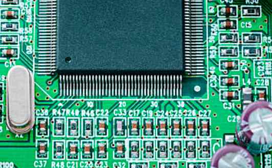
Ultra-precision six-layer PCB circuit boardwire fine, micro-hole, improve the requirements of the processing equipment control level of circuit board processing plant, but also the overall management ability of precision six-layer PCB circuit board factory and the ability of employees. 6/6mil line width/line distance manufacturing capability, within the current equipment and materials, and process control level, without too much difficulty, most PCB manufacturers can produce. But from 6/6mil to 5/5mil, is a big leap, many small and medium-sized manufacturers hope to sigh. Seemingly simple, in fact, this requires circuit board manufacturers have strong technical research and development ability and financial strength. Subject to the performance parameters of the exposure machine, etching line processing capacity, as well as the control ability of the whole process, to achieve 5/5mil line, and maintain a high yield, need the strong overall strength of the factory to support. The same is true for the finished aperture of 0.3mm and below (holes below 0.3mm cannot be drilled by machine, generally laser drilling).
The importance of PCB as an electronic element carrier
As the carrier of all electronic components, PCB reliability is very important. A small hair, a tiny particle of dust, can lead to the entire PCB board scrap, or lead to potential failure. So how is quality guaranteed? It is generally assumed that quality should be manufactured, but it is not. If a PCB factory from the beginning of design, including factory layout, process determination, production equipment selection, manpower allocation, effective evaluation of raw materials, management system determination and other aspects, from the perspective of effective quality control, make corresponding adjustment and control, and prevention of common quality problems, and give full consideration to improve production efficiency, Then the quality control ability and production capacity of this factory in the future will have a good foundation and guarantee.
What should be prepared in advance before pcb board proofing
Generally, pcb board proofing will be done for testing before doing experiments or mass production of pcb board. There are many forms of pcb files. In order to meet different market needs, pcb board manufacturers can open these different forms of files. Then, what materials need to be prepared before pcb board proofing? Follow along to find out!
In general, pcb or GERBER files need to be provided to pcb manufacturers, which should include some board making instructions, such as the number of board sub-layers, required material, pad process, ink color and other specific production requirements. Specific instructions are as follows:

1. Materials: To explain what materials are needed to produce pcb, FR4 is commonly used, and the main material is epoxy resin stripped fiber cloth board.
2. Board layer: After pcb board proofing, the number of layers has an impact on the price, so it is necessary to indicate how many layers of board to be made.
3. Welding resistance color: the conventional color is green, other colors need to be indicated.
4. Screen printing color: screen printing font and frame color on pcb board, the default choice is generally white.
5, copper thickness: generally according to the circuit current to scientific calculation of the thickness of copper, generally the thicker the better, but the cost will be higher, so the need for a reasonable balance
Whether the hole is covered by solder resistance: The solder resistance is to insulate the hole, otherwise it is to let the hole is not insulated.
6, surface coating: pcb board before proofing to explain the surface coating is spray tin or gold plating.
7. Quantity: The quantity of pcb should be clearly stated.
The above is the data to be prepared before pcb board proofing, I hope to help you!


