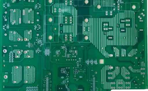
High-speed circuits need to place their components as close together as possible to achieve short, direct signal paths, but they are not components that have this requirement. Analog circuits and power supply assemblies also need to be placed to make their sensitive or high-current lines as short as possible. This helps reduce inductance and improves signal and power integrity. However, in some cases, these components may need to be separated to accommodate bus wiring or thermal separation.
manufacturability
To keep production costs as low as possible, it is important to place components in a way that is as easy to manufacture as possible. For example, components that are too close to each other may not be assembled automatically, or it may be difficult to use automatic welding processes. Wave soldering of taller chip components before smaller components creates a shadow effect, resulting in poor welded connections. Uneven copper between the two pads of a small chip assembly creates uneven heating, causing the solder in one pad to melt before the other and pulling the other side up away from the pad.
barrier-free
Boards often have to be manually tested and reworked, which requires access to the parts that need to be handled. If these parts are obscured by other larger components, it can make their work more time-consuming or cause collateral damage to adjacent parts. Likewise, connectors, switches, and other inaccessible human interfaces can slow down the manufacturing of boards.
An extremely important guideline is that the layout should start with a basic floor plan of the components on the development board. This will allow you to stratetize how to divide the different circuit areas on the board to avoid overlapping analog and digital signals.

PCB Layout Guide: Effective component placement will result in wire routing
Guidelines for PCB design and layout of wiring
It is critical for board designers to lay out their boards to create the best possible signal and power integrity. Components shall be placed in a good position for short and direct wiring. At the same time, the boards must be laid out so that all the networks can be fully wired. Trying to balance these requirements can be quite a challenge in high-density design. The first PCB design layout guide sets design rules and constraints for wiring.
Design rules and constraints
Technically, configuration design rules and constraints should be included in the parameters and Settings. However, since most of the rules apply directly to tracing routes, we have included this guide here. Rules and constraints are used to control cable width and spacing and can be set for a single network, a network group called a network class, or as the default for all non-specified networks. Design rules are also used to control which holes are selected for different networks, route lengths, and match lengths, and which board layers are allowed for routing specific networks and routing topologies. In addition, design rules are used to control component spacing, silkscreen rules, mechanical clearance, and many other constraints.
Signal and power integrity
In order to achieve better performance and signal integrity, PCB layout designers need to follow the specific requirements of different circuit routing. Design rules and constraints help here -- allowing the designer to enter physical wiring parameters into the CAD system for wiring. Although the exact value can vary depending on the needs of the board, designers often set rules to ensure that the following guidelines are followed:
Short and direct high-speed transmission line routing.
Line width, spacing, and allowable layers for controlled impedance wiring.
Match the specified line length and length tolerance of the length wiring.
Difference requirements for cable width and spacing.
Width and spacing of sensitive signals such as clocks and control lines.
Orifice types of different networks.
Line width and spacing of analog circuits.
High current power supply circuit line width and copper weight.
Another important guideline to keep in mind is to avoid areas where digital circuits cross analog wiring and vice versa when wiring in a mixed-signal design.
Guide to effective power supply and ground plane


