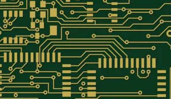
Printed circuit board develops from single layer to double panel, multilayer board and flexible board, and continuously develops to high precision, high density and high reliability direction. Constantly reduce the size, reduce the cost, improve the performance, so that the printed circuit board in the future of the development of electronic products, still maintain strong vitality.
The development trend of PCB manufacturing technology in the future is to high density, high precision, fine aperture, fine wire, small spacing, high reliability, multi-layer, high-speed transmission, light weight, thin shape.
Factors that may lead to holes in the process before metallization of PCB circuit boards: three factors that lead to holes in the processing of PCB circuit boards
The first factor: drilling
A worn bit or other improper drilling parameters may tear the copper foil and dielectric layer, creating cracks. Glass fibers can also be torn rather than cut. Whether the copper will tear from the resin depends not only on the quality of the borehole, but also on the strength of the bond between the copper foil and the resin. A typical example is that the bonding between the oxide layer and the semi-cured sheet is often weaker than that between the dielectric substrate and the copper foil, so most tearing occurs on the surface of the oxide layer of the multilayer. In gold, tearing occurs on the smoother side of copper foil unless it is "revers treated foil." Poor bonding of the oxide surface to the semi-cured sheet can also lead to a worse "pink ring", where the oxide layer of copper dissolves in the acid.

Rough hole walls or rough hole walls with pink rings will lead to holes at the multi-layer junction, called wedge holes or blow holes," wedge holes "initially at the junction, its name also suggests: shaped like a" wedge ", retraction to form a cavity, usually can be covered by electroplating. If the copper layer covers these ditches, there will often be moisture behind the copper layer. In later PCB processes, such as hot air conditioning and high temperature treatment, moisture (moisture) evaporation and wedge holes usually occur together. It can be easily identified and distinguished from other types of voids by their location and shape.
Second factor: decontamination/denting
Decontamination step is to remove the resin greasy stain on the inner copper by chemical method. The stain was originally caused by drilling. Cavitation is the further deepening of decontamination, which is to remove more resin, so that copper "protrude" from the resin, and form "three-point combination" or "three-side combination" with the copper plating layer, to improve the interconnection reliability. Permanganate is used to oxidize resins and "etch" them.
The resin first needs to be swollen so that it can be treated with permanganate. The neutralization step can remove the manganese residue. The glass fiber is etched using a different chemical method, usually hydrofluoric acid. Improper decontamination can result in two types of cavities: rough resin fouling on the pore wall may contain liquid, which can lead to "blow holes". Residual muck on the inner copper layer can prevent good bonding of the copper/copper coating, resulting in "hole wall pullaway", such as separation of the copper coating from the hole wall during high temperature treatment, or related testing. Resin separation may lead to pore wall pulling and cracking and cavity in copper plating layer. If the potassium manganate residue is not completely removed in the neutralization step (to be precise 5, when it is a reduction reaction), it may also lead to cavitation. Reduction reactions often use reducing agents, such as hydrazine or hydroxylamine.
The third factor: catalytic steps before chemical copper deposition
The mismatch between decontamination/erosion/chemical copper deposition and the inadequacy of the individual steps are also worth considering. Those who have studied voids in pores strongly endorse the unified integrity of chemical treatment. The traditional pretreatment sequence of copper deposition is cleaning, adjusting, activating (catalytic), accelerating (post-activating), and entering into the cleaning (leaching), preleaching, which is completely suitable for Murpiy principle. For example, the regulator, a cationic polyester electrolyte used to neutralize the negative charge on glass fibers, often has to be applied correctly to get the required positive charge: too little regulator, poor activation layer and adhesion; Too much adjustment agent, will form a layer of film resulting in poor adhesion of copper deposition; So that the wall of the hole pulls away.
Regulator coverage is not sufficient, most likely to appear in the glass head. In metallography, hollow openings appear in glass fibers with poor copper coverage or no copper. Other causes of the cavity in the glass are: insufficient glass etching, resin etching too much, glass etching too much, insufficient catalysis, or the activity of the copper sink is not good. Other factors affecting the coating of Pcb activated layer on pore wall include: activation temperature, activation time, concentration, etc. If the cavity is on the resin, there may be the following reasons: manganate residue from the decontamination step, plasma residue, inadequate adjustment or activation, and low activity of the copper sink.


