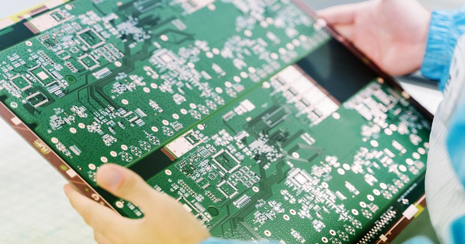
These electronic products are designed to save space and make products lighter and more compact. Durable and to obtain good performance, the previous wire connection must be removed and switched to the printed circuit board. PCB meets the requirements of space, performance and reliability.

Not every appliance needs a circuit board. Simple appliances may not need a circuit, such as a motor. However, electrical appliances with specific functions usually need circuit boards, such as televisions, radios, computers, etc. There is also a PCB at the bottom of the rice cooker and a governor in the fan.
What other types of products can be used for PCB boards?
PCB board usually refers to hard circuit board, which is mainly used for: computer motherboard, mouse board, graphics card, office equipment, printer, copier, remote controller, various chargers, calculators, digital cameras, radio, TV motherboard for household appliances, limited TV amplifier, mobile phone, washing machine, electronic scale, telephone, LED light, etc.: air conditioner, refrigerator, stereo, MP3; For industrial equipment: GPS, automobiles, instruments, medical instruments, aircraft, military weapons, missiles, satellites, etc.
The main board and keyboard of the mobile phone are hard boards; The connecting cable of the slide phone or flip phone is a soft board. The remote control is usually a carbon film plate. From top to bottom, the mobile phone board is composed of RF circuit, power circuit, audio circuit and logic circuit.
Pcb board design
Generally, the heated kettle does not have a circuit board, and the wire bracket is directly connected. The distributor has a circuit board. Electric rice cookers usually have circuit boards, while induction cookers also have circuit boards. The circuit board of the electric fan is usually used for speed regulation, timing, display, etc., and has no actual impact on the operation of the electric fan.
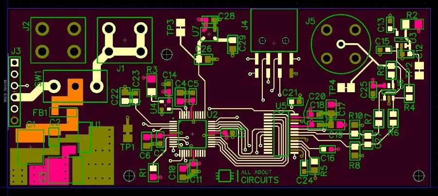
Pcb design layout
Pcb layout is a problem that designers must face first. This problem depends on certain parts of the drawing, and some devices need to be set together according to logical considerations. However, it should be noted that temperature sensitive components (such as sensors) should be placed separately from heat generating components (including power converters). For designs with multiple power settings, 12 volt and 15 volt power converters can be placed at different locations on the board because the heat and electronic noise they generate can affect the reliability and performance of other components and boards.
In the process of circuit board design, electromagnetic interference (EMI) is indeed a factor that must be carefully considered. The problem of far field electromagnetic interference (EMI) can be solved by installing filters at noise points or shielding signals with metal enclosures. However, attention should be paid to the equipment that can release electromagnetic interference (EMI) on the circuit board, thus allowing the circuit board to use a cheaper housing, thus effectively reducing the cost of the entire system.
As far as the design of multilayer circuit boards is concerned, the design of vias between different layers of circuit boards may be the most controversial issue, because the design of vias will lead to the production of circuit boards. Ask many questions. The through-hole between each layer of the circuit board will affect the performance of the signal and reduce the reliability of the circuit board design, so full attention should be paid.
Pcb board design solution
In the process of PCB design, many different methods can be used to solve various problems. It includes the adjustment of the design scheme itself, such as adjusting the circuit layout to reduce noise; And a layout method of a printed circuit board. You can use the layout tool to automatically install design components, but if you can manually adjust the automatic layout, it will help improve the quality of the board design. Through this measure, the design rule check will rely on technical documents to ensure that the circuit board design can meet the requirements of the circuit board manufacturer.
Separating the different layers of the circuit board can reduce the associated capacitance, but this will increase the number of layers of the circuit board, which will increase the cost and cause more through-hole problems. Although the orthogonal grid power system and grounding wire design may increase the physical size of the circuit board, it can effectively play the role of the grounding layer in the double-layer circuit board, thus reducing the capacitance and manufacturing complexity of the circuit board.
Design rule detection is also a very powerful tool, which can detect lines to ensure that the distance between lines is not too close, resulting in a circuit that is too short. However, the overall design still has high economic value. The design planning inspection tool can also be used to detect and adjust the power supply and ground plane to avoid large areas of related capacitance.
Pcb board design layout conclusion
Many problems need to be considered when designing a printed circuit board (PCB). Tools including DesignSpark PCB can effectively handle most of these problems. By adopting some best practice guidelines, engineering designers can effectively reduce costs, improve the reliability of circuit boards, meet system specifications, and conduct bending system certification at a lower cost, thus avoiding more problems.


