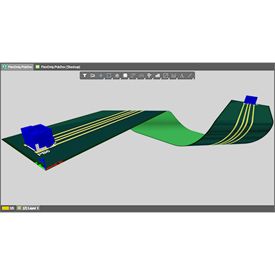
Multilayer flexible PCB design manufacturer
Name: Multilayer flexible PCB design manufacturer
Designable layers: 1-32 layers
Minimum line width and line spacing: 3mil
Minimum laser aperture: 4mil
Minimum mechanical aperture: 8mil
Copper foil thickness: 18-175цm (standard: 18цm35цm70цm)
Peel strength: 1.25N/mm
Minimum punching hole diameter: single side: 0.9mm/35mil
Minimum hole diameter: 0.25mm/10mil
Aperture tolerance: ≤φ0.8mm±0.05mm
Hole tolerance: ±0.05mm
Hole wall copper thickness: double-sided/multi-layer: ≥2um/0.8mil
Hole resistance: double-sided/multi-layer: ≤300цΩ
Minimum line width: 0.127mm/5mil
Minimum pitch: 0.127mm/5mil
Screen printing color: black, white, red, green, etc.
Surface treatment: lead/lead-free tin spray, ENIG, silver, OSP
Service: Provide OEM service
Certificate: ISO9001.ROSH.UL
Flexible printed circuits have many benefits, including:
Reduce Assembly Errors - Through precise design and automated production, flex circuits eliminate human error in manual wiring harnesses. Except for errors caused by production, circuits are routed only to those points required by the exact design plan.
Reduced assembly time and cost - Flex circuits require less labor during assembly and reduce production errors. Flexible circuits have an inherent ability to integrate form, fit and function. Flex circuits eliminate the high cost of routing, wrapping and soldering wires. Install or replace a complete interconnect system instead of individual hard PC boards. As a result, wiring errors are eliminated, thereby reducing manufacturing costs. Assembly time and cost can be reduced, whether for low-volume production of complex circuits or high-volume production of simple circuits.
Design freedom - Unlike rigid circuit boards, flex circuits are not limited to two dimensions. Because they are as flexible as wire or ribbon cables, the flex circuit design options are endless. At Flexible Circuit, we pride ourselves on being able to tackle the most complex design challenges. Flexible circuits can be designed to meet highly complex and unimaginable configurations, while being able to operate in the harshest environments.
Name: Multilayer flexible PCB design manufacturer
Designable layers: 1-32 layers
Minimum line width and line spacing: 3mil
Minimum laser aperture: 4mil
Minimum mechanical aperture: 8mil
Copper foil thickness: 18-175цm (standard: 18цm35цm70цm)
Peel strength: 1.25N/mm
Minimum punching hole diameter: single side: 0.9mm/35mil
Minimum hole diameter: 0.25mm/10mil
Aperture tolerance: ≤φ0.8mm±0.05mm
Hole tolerance: ±0.05mm
Hole wall copper thickness: double-sided/multi-layer: ≥2um/0.8mil
Hole resistance: double-sided/multi-layer: ≤300цΩ
Minimum line width: 0.127mm/5mil
Minimum pitch: 0.127mm/5mil
Screen printing color: black, white, red, green, etc.
Surface treatment: lead/lead-free tin spray, ENIG, silver, OSP
Service: Provide OEM service
Certificate: ISO9001.ROSH.UL


