Printed circuit board (PCB) layout and design services are one of the ways we help our customers get to market faster because our engineering team has extensive hands-on experience designing PCBs for performance and manufacturability.
What is included?
We are responsible for the entire cycle of the PCB design process, from PCB schematic design and PCB board layout to testing, verification and certification.
Write technical specifications
Preparing project specifications is an important part of custom PCB design services. It may include technical requirements, block diagrams, deliverables, assumptions, preliminary bill of materials (BOM) and BOM costs, tools and techniques specified for project development. This specification allows our designers to align with our clients and meet their expectations.
Schematic Design
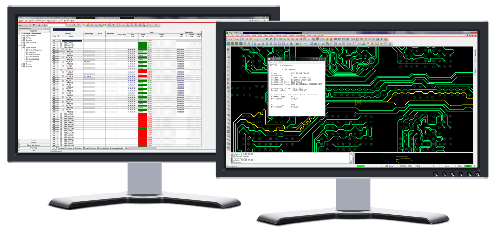
The process of PCB board design always starts with a schematic diagram. A schematic or circuit diagram conveys the electrical connections between different electrical components, such as integrated circuits (ICs) and discrete components. To provide this PCB design service, we use professional CAD software to define the modules and design the connectivity between the different components.
PCB layout
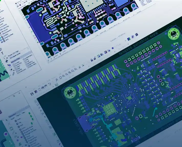
After importing the schematic into the PCB layout, we manually placed and routed the components on the board. We took into account the number of layers required and the size of components that may be limited by the size of the enclosure. In our PCB layout services, we analyze signal integrity and evaluate electrical constraints to ensure the safety of board-level architectures. For complex layouts, we incorporate various simulations into our custom board design services. Our experts arrange proper conductor routing, which is a major factor in the price of PCB manufacturing. We run DFM/DFA analysis to minimize PCB design modifications, reduce development costs, and reduce time to market.
PCB Manufacturing and Testing
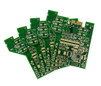
Once our PCB design layout is approved for production, we export it to a manufacturer-supported format. We prepare Bill of Materials (BOM) and Gerber files describing the design requirements for each image of the board. Manufacturers use this document as a reference for circuit board fabrication and PCB assembly. For some projects, we also created a 3D model of the PCB to make sure it would fit in the enclosure. Testing is essential for both our PCB layout design services and the manufacturing stage. We provide manufacturers with the data and software they need to perform electrical and impedance testing. After the prototype is complete, we test it in-house.
mass production
After prototype validation, we prepare documentation for mass production and assist customers throughout the manufacturing process. We arrange special software, hardware and testing procedures. Using them, manufacturers can test each PCB at the factory.
technical support
After the project was completed, we created a complete documentation package that included BOM and Gerber files, 3D models, and technical manuals. In addition, we set a warranty period for our PCB design services. During this time, we fix bugs and provide other technical support covered under warranty. After the warranty period is over, we keep in touch with the customer and consult when needed.


