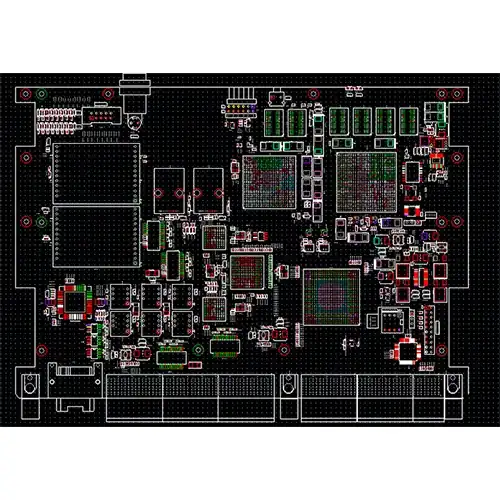
Photoelectric Multimedia PCB Design
Name: Photoelectric Multimedia PCB Design
Photoelectric multimedia circuit board design features:
Optoelectronic multimedia FPGA processor, 10G SFP optical port
Photoelectric multimedia PCB board parameters:
PCB name: 6 layers
PCB Category: Through Hole Board
PCB board: Htg170
Board size: 146.3*167.4*1.6mm
Surface Treatment: Immersion Gold Process
PCB copper thickness: 1OZ
Minimum line width: 5MIL
Minimum line spacing: 5MIL
Minimum hole diameter: 10MIL
Impedance control: +/-5%
The optoelectronic printed circuit board is a new generation of packaging substrate with high computing requirements that collects light and transmits electrical-to-optical signals and uses electricity for computing.
The optoelectronic circuit board according to the present invention is an optoelectronic circuit board in which at least a rigid portion formed and laminated with a conductor circuit and an insulating layer and one or more bendable flexible portions are integrated, an external connection portion for mounting An optical element and/or a package substrate on which the optical element is mounted is formed in the above-mentioned rigid portion, and an optical path is formed in at least one of the above-mentioned flexible portions.
Name: Photoelectric Multimedia PCB Design
Photoelectric multimedia circuit board design features:
Optoelectronic multimedia FPGA processor, 10G SFP optical port
Photoelectric multimedia PCB board parameters:
PCB name: 6 layers
PCB Category: Through Hole Board
PCB board: Htg170
Board size: 146.3*167.4*1.6mm
Surface Treatment: Immersion Gold Process
PCB copper thickness: 1OZ
Minimum line width: 5MIL
Minimum line spacing: 5MIL
Minimum hole diameter: 10MIL
Impedance control: +/-5%


