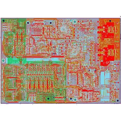
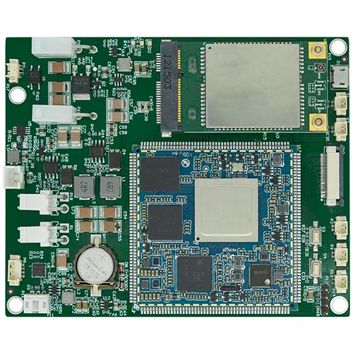
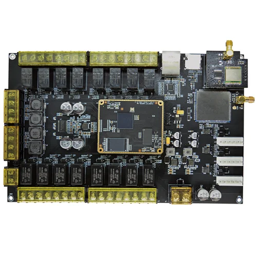
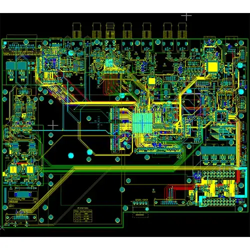
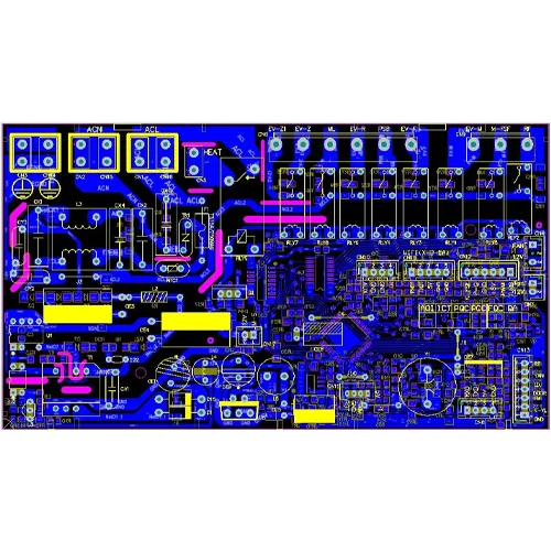
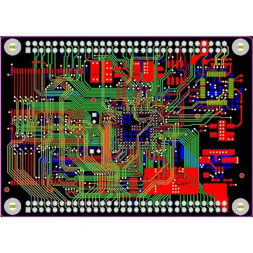
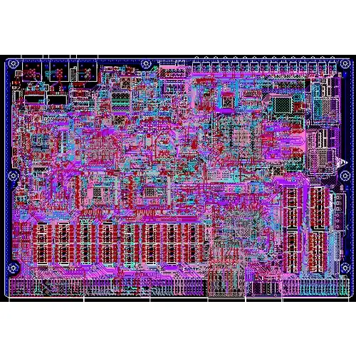
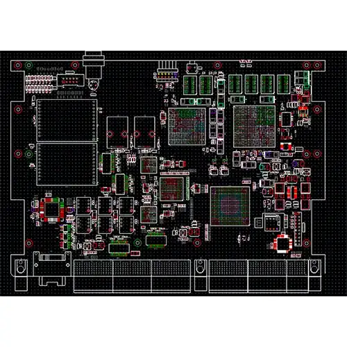
PCB design of integrated terminal
Name: PCB design of integrated terminal
Integrated terminal PCB design features:
1. Multi-module, dual-system system, powerful,
2. HiSilicon image coding comes with Android system,
3. Rockchip image decoding comes with Linux system.
PCB board parameters:
Number of PCB layers: 8 layers
PCB material: Htg170
PCB size: 185*124.5*1.6mm
Surface Treatment: Immersion Gold Process
PCB copper thickness: 1OZ
Minimum line width: 4MIL
Minimum line spacing: 4MIL
Minimum aperture: 8MIL
Impedance control: +/-10%
What are PCB terminals?
PCB terminal blocks are modular insulating devices that mount on a printed circuit board (PCB) and hold two or more wires together. Terminal blocks are used to hold and/or terminate electrical wires and in their simplest form consist of multiple individual terminals arranged in long strips.
PCB terminal blocks make it easy and safe to transfer signals, data and power to the PCB. They are suitable for a wide variety of applications in numerous industries, markets and Industry 4.0 applications. Our COMBICON range of XS to XXL product lines includes metric and imperial pitch, from 2.5mm pitch miniature terminals to 20mm pitch power stage terminals.
Name: PCB design of integrated terminal
Integrated terminal PCB design features:
1. Multi-module, dual-system system, powerful,
2. HiSilicon image coding comes with Android system,
3. Rockchip image decoding comes with Linux system.
PCB board parameters:
Number of PCB layers: 8 layers
PCB material: Htg170
PCB size: 185*124.5*1.6mm
Surface Treatment: Immersion Gold Process
PCB copper thickness: 1OZ
Minimum line width: 4MIL
Minimum line spacing: 4MIL
Minimum aperture: 8MIL
Impedance control: +/-10%
- Previous:Photoelectric Multimedia PCB Design
- Next:No


