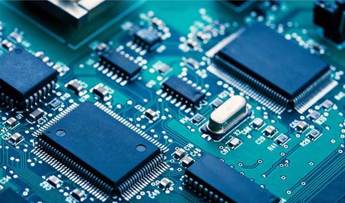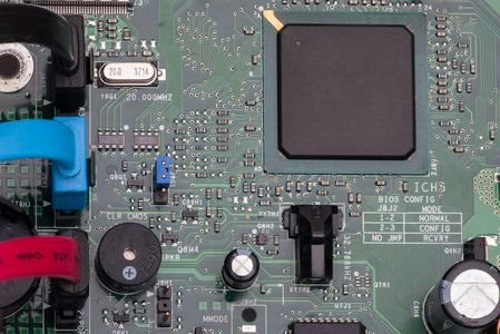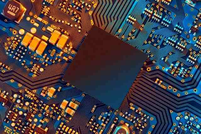
The basic characteristics of printed circuit board depend on the performance of the substrate board, to improve the technical performance of printed circuit board must first improve the performance of printed circuit substrate board, in order to meet the needs of the development of printed board, a variety of new materials are gradually developed and put into use.
In recent years, PCB market focus has shifted from computer to communication, including base station, server and mobile terminal, etc. Mobile communication equipment represented by smart phone drives PCB to higher density, thinner and higher function development. Printed circuit technology cannot be separated from the substrate material, which also involves the technical requirements of the substrate used in PCB circuit board.
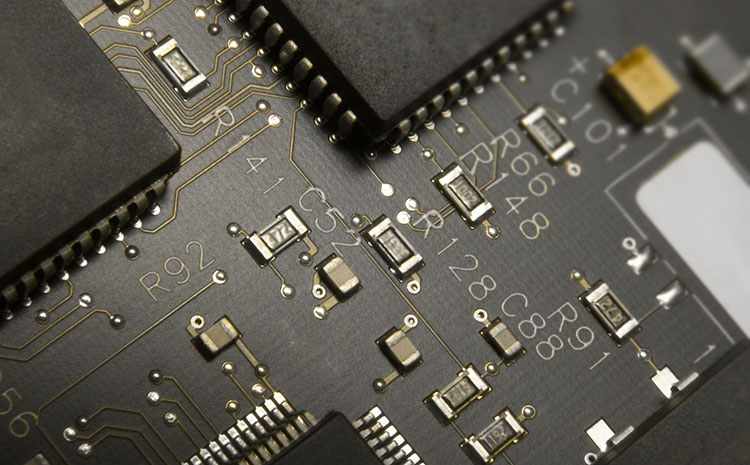
High density fine line demand
PCB board all to high density fine line development, HDI board is particularly prominent. Ten years ago IPC for HDI board under the definition of line width/line distance (L/S) is 0.1mm/0.1mm and below, now the industry basically do conventional L/S for 60μm, advanced L/S for 40μm. PCB circuit pattern formation, the traditional copper foil substrate after photoimaging chemical etching process (reduction method), the reduction method of fine line production limit is about 30μm, and need to use thin copper foil (9~12μm) substrate. Due to the high price of thin copper foil CCL and the high lamination defects of thin copper foil, many factories produce 18μm copper foil and then use etching to reduce the copper layer in production. This method has many processes, difficult thickness control and high cost. It is better to use thin copper foil. In addition, PCB circuit board line L/S is less than 20μm, the general thin copper foil is also difficult to do, need to use ultra-thin copper foil (3~5μm) substrate and attached to the carrier ultra-thin copper foil.
The current fine line requirements of copper foil in addition to thinner thickness, at the same time need copper foil surface roughness. In order to improve the binding force between copper foil and substrate and ensure the stripping strength of conductor, coarsening of copper foil layer is usually adopted. The conventional copper foil roughness is greater than 5μm. Copper foil rough convex peak embedded in the substrate is to improve the stripping resistance, but in line etching to control wire precision is not too etching, it is easy to embed the substrate convex peak residue, resulting in short circuit between the lines or insulation decline, especially for fine lines. Copper foils with low roughness (less than 3μm) and even lower roughness (1.5μm) are required. However, the roughness of copper foil decreases while the anti-stripping strength of the conductor still needs to be maintained. Special treatment is needed for the surface of copper foil and substrate resin. If there is a smooth resin surface electroless plating copper foil with high binding force; If there is "molecular bonding technology", is the chemical treatment of the surface of the resin substrate to form a functional group can be closely combined with the copper layer.
Requirements for laminated insulating dielectric sheets
HDI board technology is characterized by the integration process, commonly used resin coated copper foil, or semi-cured epoxy glass cloth and copper foil lamination layer is difficult to reach fine lines. Now tends to use the semi-addition method or improved semi-processing method, that is, the use of insulating medium film layer, and then electroless copper plating to form a copper conductor layer, because the copper layer is extremely thin and easy to form fine lines.
One of the key points of the semi-addition method is the laminated dielectric material. In order to meet the requirements of high density and fine lines, the laminated material is proposed to meet the requirements of dielectric electricity, insulation, heat resistance, binding force and so on, as well as the process adaptability with HDI board. At present, ABF/GX series products of Ajinomoto Company are the main HDI stacking medium materials in the world. Epoxy resin is combined with different curing agents, inorganic powder is added to improve material rigidity and reduce CTE, and glass fiber cloth is also used to enhance rigidity. A similar thin film lamination material was developed by the Japanese Water Chemical Company and by the Taiwan Institute of Industrial Research. ABF materials also continue to improve and develop, the new generation of laminated materials in particular requires low surface roughness, low thermal expansion rate, low dielectric loss and thin hardening.
In semiconductor packages around the world, IC packaging boards have been replaced by organic substrates instead of ceramic ones. Flip chip (FC) packaging boards have increasingly smaller pitch, with typical line width/line spacing now 15μm, and will be thinner in the future. The performance of multilayer carrier plate requires low dielectric property, low thermal expansion coefficient and high heat resistance, and low cost substrate is pursued on the basis of meeting the performance objectives. At present, the mass production of fine line basically adopts the MSPA process of insulating medium layer combined with pressed thin copper foil. SAP method is used to fabricate circuit patterns with L/S less than 10μm.
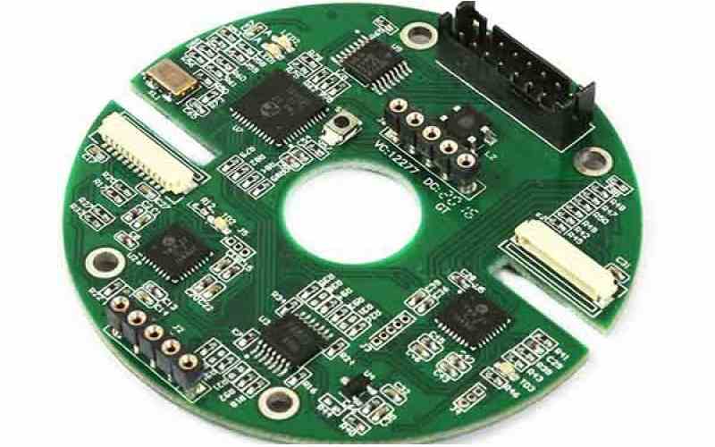
When PCB board is thicker and thinner, HDI board technology develops from core-containing layer to non-core-containing Anylayer. The area and thickness of HDI board with the same function can be reduced by about 25% compared with that of HDI board with core-containing layer. These must use thinner dielectric layers that retain good electrical properties.
High frequency and high speed demand
At present, the high frequency circuit board substrate is mainly fluorine resin, polyphenyl ether (PPO or PPE) resin and modified epoxy resin these three categories of materials. Fluorinated dielectric substrates, such as polytetrafluoroethylene (PTFE), have the lowest dielectric properties and are usually used above 5GHz. In addition, modified epoxy FR-4 or PPO substrates can be used for products between 1GHz and 10GHz. Among these three types of high-frequency substrate materials, the cost of epoxy resin is the cheapest, while fluorine resin is the most expensive; From the dielectric constant, dielectric loss, water absorption and frequency characteristics, fluorine resin is the best, epoxy resin is worse. When the product application frequency is higher than 10GHz, only fluorine resin printed board can be suitable. But the disadvantages of PTFE are poor rigidity and high coefficient of thermal expansion in addition to high cost.
For polytetrafluoroethylene, in order to improve the performance with a large number of inorganic filler materials or glass cloth for reinforcement, to improve the rigidity of the substrate and reduce its thermal expansion. In addition, because of the molecular inertia of PTFE resin itself, it is not easy to combine with copper foil poor, so it is more necessary to combine with copper foil special surface treatment. Treatment methods on the surface of PTFE chemical etching or plasma etching, increase the surface roughness or add a layer of bonding film between copper foil and PTFE resin to improve the bonding force, but may have an impact on the performance of the medium, the whole fluorine system high frequency electric subgrade board still needs to be further developed.
In addition to the special requirements for insulating materials such as resin, the surface roughness of conductor copper is also an important factor affecting signal transmission loss, which is affected by skin effect. The skin effect is the electromagnetic induction generated in the wire during the transmission of high-frequency signals. The inductance is larger at the center of the cross section of the wire, so that the current or signal tends to be concentrated on the surface of the wire. Conductor surface roughness affects the transmission signal loss, smooth surface loss is small.
At the same frequency, the greater the surface roughness of copper, the greater the signal loss, so we try to control the surface roughness of copper thickness in the actual production, the smaller the roughness without affecting the binding force, the better. Especially for signals in the range above 10GHz. The copper foil roughness at 10GHz should be less than 1μm, and the superplane copper foil (surface roughness 0.04μm) is better. Copper foil surface roughness also needs to be combined with appropriate oxidation treatment and bonding resin system. In the near future, there will be a nearly contourless resin coated copper foil, can be higher peel strength without affecting dielectric loss.

High heat resistance and heat dissipation requirements
With the miniaturization and high function of electronic equipment, high heating is generated, and the thermal management requirements of electronic equipment are increasing. One of the solutions chosen is the development of thermal conductive printed circuit boards. Heat and heat dissipation The primary condition of PCB board is the heat resistance and heat dissipation of the substrate. At present, the heat resistance and heat dissipation of the substrate are improved to a certain extent through the improvement of resin and the addition of filler, but the improvement of thermal conductivity is very limited. Typical is the use of metal substrate or metal core printed circuit board, play the role of heat dissipation components, than the traditional radiator, fan cooling to reduce the volume and cost.
Aluminum is a very attractive material, it is rich in resources, low cost, good thermal conductivity and strength, and environmentally friendly, metal substrate or metal core is mostly metal aluminum. Aluminum based circuit boardhas the advantages of simple economy, reliable electronic connection, high thermal conductivity and strength, welding and lead-free environmental protection, from consumer goods to automobiles, military and aerospace can be designed and applied. There is no doubt about the thermal conductivity and heat resistance of metal substrate, the key lies in the performance of the insulating binder between metal plate and circuit layer.
At present, the driving force of thermal management focuses on LED. Nearly 80% of the input power of LED is converted into heat. Therefore, the thermal management problem of LED is highly valued, with the focus on the heat dissipation of LED substrate. The composition of high heat resistance and environmental protection heat insulation layer materials lays the foundation for entering into the high brightness LED lighting market.


