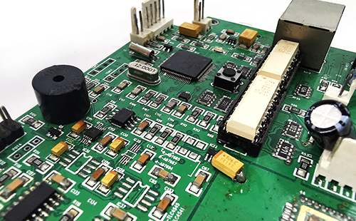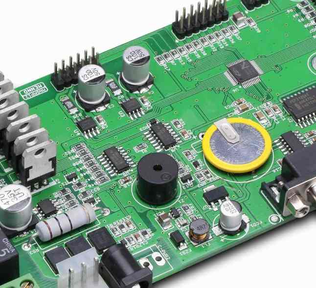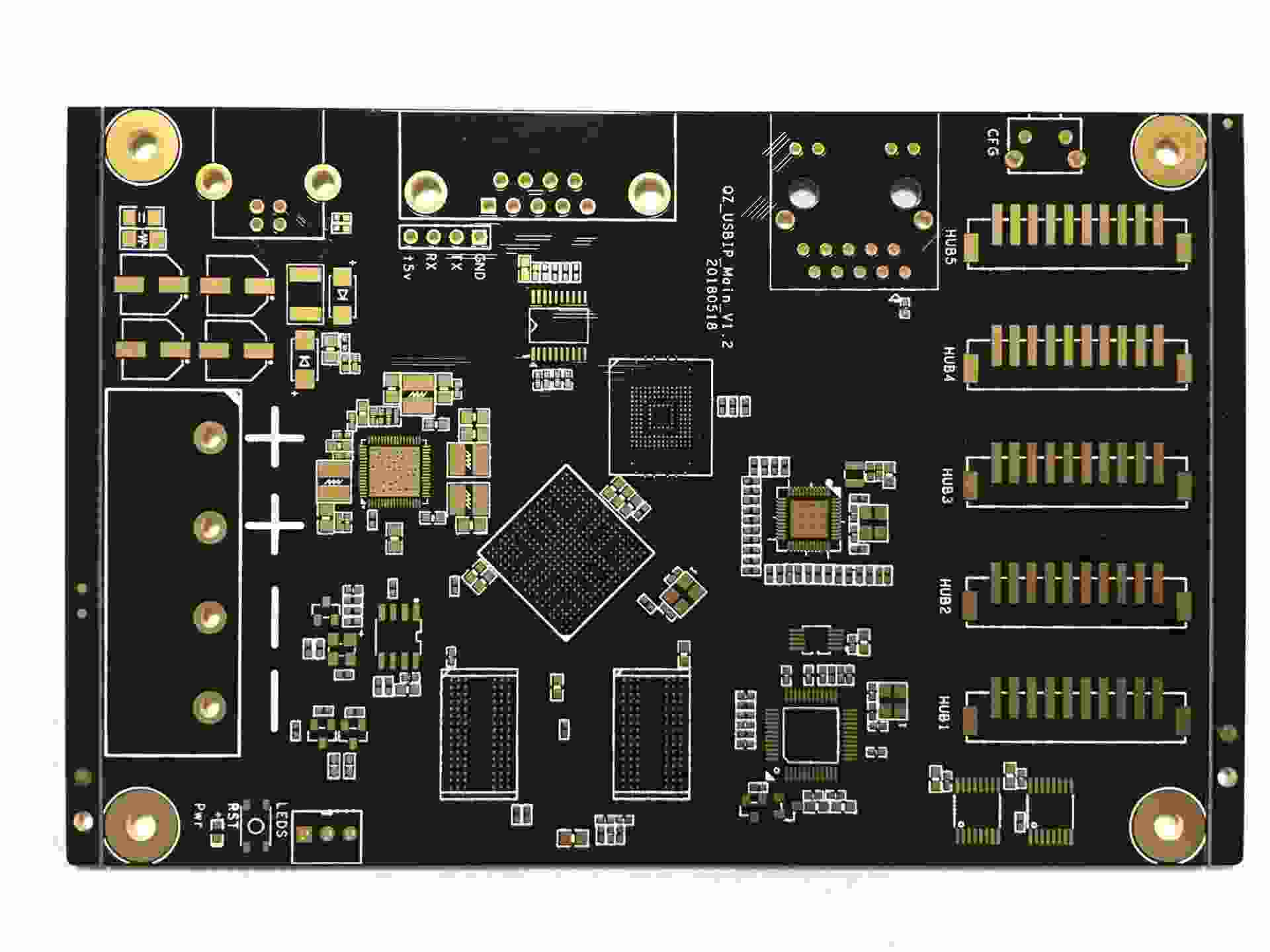
Advantages: Low cost, flat appearance, excellent weldability (in the case of no oxidation).
Defects: It is simply affected by acid and humidity, and cannot be kept for a long time. After unpacking, it needs to be used up within 2 hours, because the copper is exposed to simple oxidation in the air. Cannot be used on double panels because the second side is already oxidized after the first reflow welding. If there is a test point, the solder paste must be printed to avoid oxidation, otherwise it will not be able to touch with the probe.
HASL, Hot Air Solder Levelling, hot air solder levelling)
Advantages: Low price, good welding function.
Defects: It is not suitable for welding pins with thin gaps and too small components, due to the poor appearance flatness of the tin-spraying plate. In the PCB processing, solder bead is simple to form a short circuit for fine pitch components. When applied to double-sided SMT process, because the second side has been through a high temperature reflow welding, it is very simple to melt the tin spray from scratch, and the tin beads or similar water beads are affected by gravity into dripping spherical tin spots, forming more uneven appearance and thus affecting the welding problem.
Tin spraying process used to be the dominant process in PCB surface treatment. But the tin-spraying process is excellent for larger components and wider-spaced wires. In PCB circuit boards with high density, the flatness of tin-spraying process will affect the subsequent assembly. Therefore, the HDI circuit board generally does not use the tin spray process. With the progress of technology, the industry has now presented a suitable for assembling smaller spacing of QFP and BGA tinspray process, but the practice is less.
OSP(Organic Soldering Preservative)
Advantages: With all the advantages of bare copper plate welding, expired (three months) of the board can also be done from scratch, but generally only once.
Defects: Simply affected by acid and humidity. When used in secondary reflow welding, it needs to be completed within a certain time, and generally the role of the second reflow welding will be relatively poor. Storage time if more than three months must be dealt with from scratch. It should be used within 24 hours after unpacking. OSP is the insulating layer, so the test point must be printed with solder paste to remove the original OSP layer before touching the pin point for electrical test.
OSP process can be used in low technology content of PCB circuit boards, can also be used in high technology content of PCB circuit boards, such as single-side TV PCB circuit boards, high density chip sealing machine boards. In terms of BGA, OSP is also used more. The OSP process is the most ideal external processing process for PCBS, provided that there are no external interface functional requirements or storage life limits. But OSP is not suitable for use in a small number of diverse products, also not suitable for use in the demand of the estimated products, if the company's inventory of circuit boards often more than six months, really do not advocate the use of OSP appearance processing board.
ENIG, Electroless Nickel Immersion Gold (ENIG, Electroless Nickel Immersion Gold)
Advantages: not easy to oxidize, can be stored for a long time, flat appearance, suitable for welding fine gap pins and small solder joint components. There are key PCB board preferred. Being able to repeat reflow more than once is less likely to reduce weldability. Can be used as the base material for COB(Chip On Board) wire.
Defects: High cost, poor welding strength, due to the use of nickel-free plating process, simple black disk. The nickel layer oxidizes over time, and long-term reliability is a problem.
Different from OSP process, it is mainly used in the appearance of the interface functional requirements and long storage life of the board, such as key contact area, router housing marginal interface area and chip processor elastic interface electrical touch area. Due to the flatness of the tin spray process and the removal of the flux in the OSP process.

It is often found that friends will be confused about the gold sinking and gilding process. Let's compare the differences and applicable scenarios between the gold sinking process and gilding process
The crystal structure formed by gold plating and gold plating is different, the gold plating plate is easier to weld than the gold plating plate, will not form poor welding;
As long as there is nickel gold on the solder plate, the skin effect signal transmission is in the copper layer will not affect the signal;
Gold-sunk circuit board is denser than gold-plated crystal structure and is not easy to oxidize;
Only support the selection of a link when the effective gold-plating circuit board as long as there is nickel gold on the pad, will not occur gold wire formation is short;
Gold-sunk circuit board as long as there is nickel gold on the plate, the line welding and copper layer combination more solid;
Sunken gold is golden, more yellow than gold and more beautiful;
Gold board is softer than gold, so it is not as good as gold board in wear resistance, and gold finger circuit board will be better.
ENIG, Electroless Nickel Immersion Gold
Sunk silver circuit board is cheaper than sunk gold, if the PCB circuit board has the functional requirements and the demand to reduce the cost, sunk silver is a good choice; With the outstanding flatness and touch of silver sinking, it is more appropriate to choose the silver sinking process.


