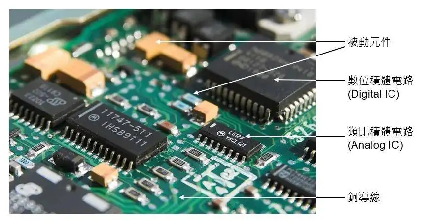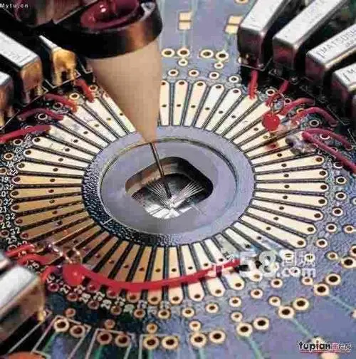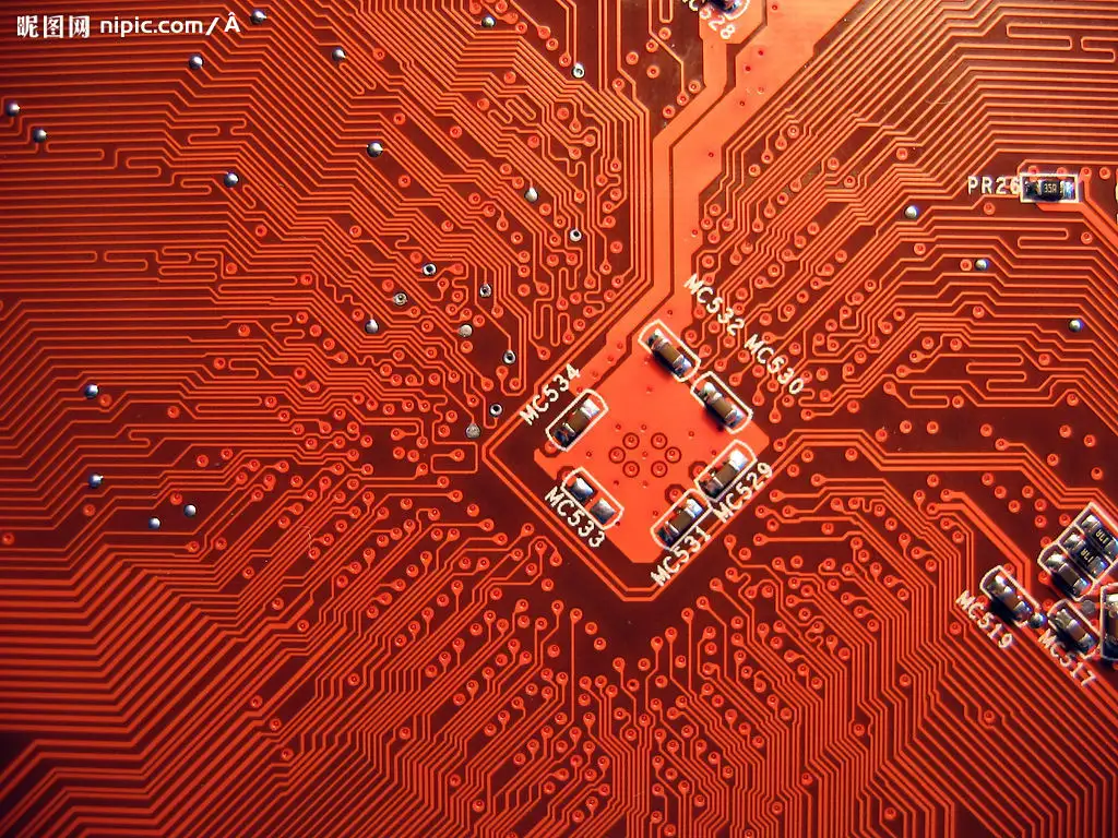
Printed circuit boards (PCBS) are the basis of every electronic device. However, in order for PCBS to work reliably, there are some best practices that must be followed during assembly. Follow these six steps to make your next PCB assembly process smoother: 1. Proper Communication
First, you need to ensure clear communication with your PCB assembly partners -- you certainly don't want to be in the position of assembling a PCB without considering your needs. You must ensure that PCB partners are aware of your customization requirements. Experienced partners are also equipped with industry best practices and will provide you with important tips, whether on improving technology, material selection, the latest trends, or all of the above. This, in turn, ensures that you don't have to reinvent the wheel.

2. DFM check
An important way to ensure that your PCB works error-free and seamlessly is to run Design for Manufacturing (DFM) tests. This test identifies any errors in the design early on and avoids costly errors and delays in processing later. Issues such as spacing between components, component polarity, footprint verification, etc., can be identified in a timely manner. In addition, DFM testing helps:
Reduce the cost
Speed up delivery and save rework time
Improve product quality
It is important that DFM testing be performed by experienced, detail-oriented engineers.
3. Check the assembly materials
The quality of the components used in a PCB is critical. When you work with a professional PCB assembler, you will benefit from their quality control department that evaluates incoming materials. Multiple factors -- such as date code, quality, and model number -- need to be verified to see if BOM matches, and various tests are performed, including:
The sample test
Check for deformed, oxidized or any damaged parts
4. Screening of SMT solder paste
The application of solder paste is a very important aspect of PCB assembly process. It is usually done by a machine that uses a mechanical fixture to attach the template to the circuit board. This is followed by an applicator that spreads solder onto the open space where the surface mount (SMT) assembly is to be held.
It is important to ensure that the solder paste composition is correct for the SMT components they are assembling. After applying solder paste, the engineer checks the circuit board to ensure that the application is correct and sufficient to secure the components.
5. X-ray examination
Another best practice is to perform an X-ray after the reflow welding process to detect quality defects and other defects. This approach is especially useful for layered and complex PCBS. The X-ray process helps to identify defects, such as:
Reflux curve error
Insufficient solder paste
Improper component placement, etc. 6. Final inspection
A professional PCB assembler will perform rigorous inspections to ensure that the PCB is fully functional and error-free. At this stage, automatic optical detection (AOI) - which uses a camera to detect faults - is often applied. AOI can help you scan a large number of PCBS in a short time.
Manual inspection is also effective for small batches of PCBS, but requires a lot of time and effort. The final inspection may also include other tests, such as online tests and functional circuit tests.
It is not easy to make circuit boards. Some gadget enthusiasts like to design and create their own printed electric boards, but they don't like the finished aspects of the machine. Besides, it takes a lot of time to make a lot of boards at home. Let us know during the circuit board assembly process to give you a better idea of how the device is created in detail.
As long as you fuse the electronic device to the printed circuit board, assemble and fabricate it. However, the panel assembly differs from its manufacture. Along with PCB production, there are several steps involved, including designing the PCB and prototyping the PCB.
It is very important to collect all the correct equipment and install it on the board before plugging in the electronics. The question now arises as to what PCB is installed in which device. Different electronic boards have different components involved, depending on what is to be installed on the device. There are two main types of manufacturing methods involved in making PCB assemblies:
1) Hole through method: In this method, the device is implanted into the hole
2) Surface mount method: In this method, the external plane of the electronic circuit board mounted on the device.
The device is mounted on a printed circuit board with the help of metal solder through the use of electricity. The capacity of the board determines how the device must be fused on the board. In the case of manufacturing a larger number of board components, it is always best to use the machine. The circuit is placed on the machine by wave soldering as well as by using a reflow furnace. Bulk wave soldering or reflow soldering furnace is placed on the machine. In the case of small-scale production, hand welding is always an option.

Sometimes the two hole through method as well as the surface mount method are applied in a single assembly, because some electronic components are only available in the hole through the sleeve, while others are only available in the surface mount package. The method was used in the assembly process when it proved to be advantageous.
Mounting holes through powerful electronic components, in case they have certain physical damage. However, it is better to make use of the surface mount method when you know that any damage is unlikely to occur. The surface mount method uses an electronic board with less area.
As long as the assembly process, it is important to check that the motherboard is working properly and performing the required functions. In the case of a fault on a part of the printed circuit board, it is easy to identify the problem and the source of replacement can be done.
Chilag Patel is a creative content writer who works on Muncie research. He blogs PCB design, consumer electronics, automotive electronics and many more.
conclusion
Advanced technology creates better PCB testing to determine accuracy and reliability. Some of the best practices mentioned above ensure that the PCB assembly process becomes seamless. Importantly, choosing a professional PCB assembler can make a significant difference when building high quality PCBS.


