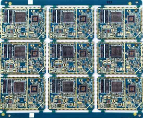
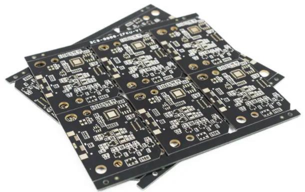
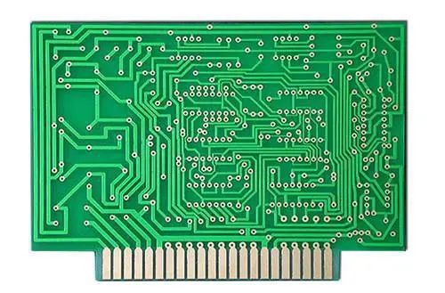
Share and explain 4 expensive PCB design errors
PCB processing factory explanation: PCB design may be extremely complex, and mistakes made at this stage of the electronic design process may cause high costs.


PCB processing factory explanation: PCB design may be extremely complex, and mistakes made at this stage of the electronic design process may cause high costs.
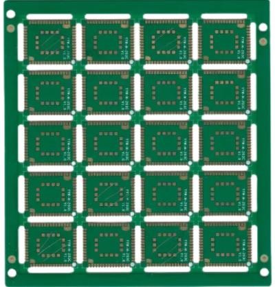
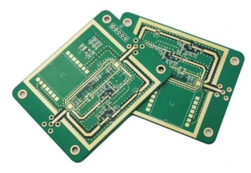
Circuit board processing factory explains how to use excellent circuit board design technology to create the best circuit board
The PCB processing factory explains all the information about PCB tool holes in pcb design: their purpose and location, and some basic rules should be followed when placing the tool holes.
PCB processing factory shares: the best practices and precautions in PCB design are explained in detail, and each PCB design can be optimized for specific applications
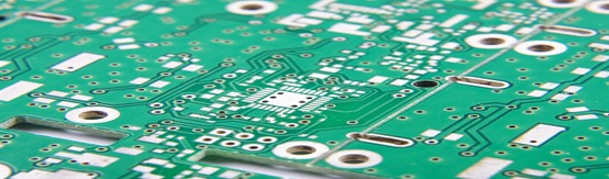
The PCB processing factory explains and analyzes the effective PCB wiring width and spacing of PCB design
Explanation of PCB processing factory: setting HDI PCB layout and wiring in PCB design software
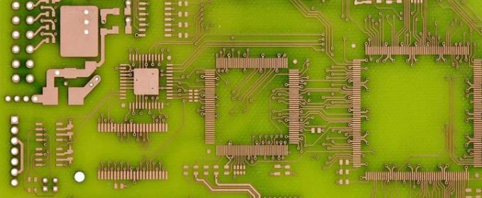
PCB processing and PCB assembly plants explain PCB wiring rules for single ended signals and PCB wiring rules for differential signals
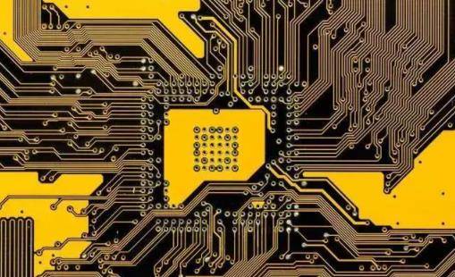
PCB processing factory explains: What is crosstalk in high-speed PCB design? How to eliminate crosstalk and potential crosstalk?

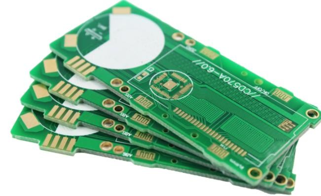
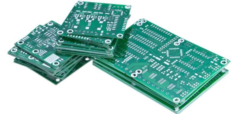
The circuit board processing factory explains the best skills of designing a multilayer PCB and arranging a multilayer PCB
Circuit board processing, circuit board assembly and processing factory explained how to change PCB reference plane during multi-layer circuit board wiring
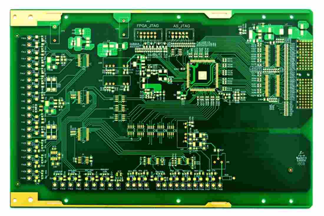
The circuit board processing factory explains what tools are needed for circuit board design, and what tools each designer needs to master
Circuit board processing factory explains the detailed sharing of digital, analog and grounding in PCB layout, and different types of grounding involved in PCB design


