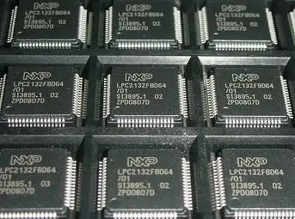
The Aspect Ratio of PCB Design and Its Importance to Multilayer PCB
Circuit board processing, circuit board assembly factory explain the aspect ratio of circuit board design and its importance to multi-layer PCB


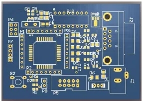
Circuit board processing, circuit board assembly factory explain the aspect ratio of circuit board design and its importance to multi-layer PCB
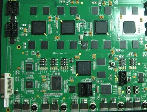
PCB assembly and processing plants share PCB design through aspect ratio: design, signal integrity and manufacturability
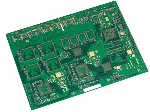
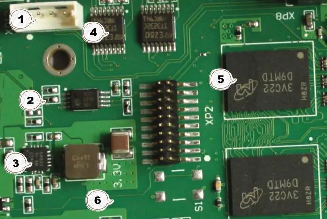
PCB assembly and PCB design factory explain the design of annular ring and multilayer PCB: keep within the tolerance range, annular connection strength: via and multilayer PCB
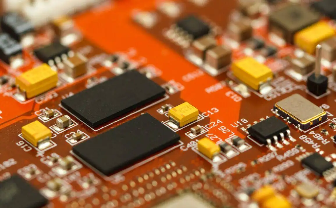
The circuit board manufacturer explains that preventing power supply integrity and signal integrity is essential for your PCB design to be smooth and static free.
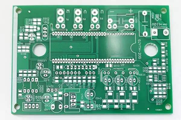
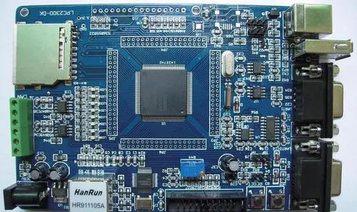
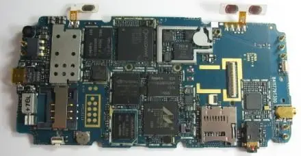
Understand PCB design, PCB assembly and PCB layout in PCB related industries, and Describe the doubts related to PCB design
Understand PCB design, PCB assembly and PCB layout in PCB related industries, and High frequency board signal design layout points and proofing
Understand PCB design, PCB assembly and PCB layout in PCB related industries, and Exploring the Four Elements of PCB Impedance Board Design
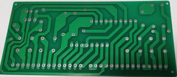
Understand PCB design, PCB assembly and PCB layout in PCB related industries, and Describe PCB board etching and resist film peeling design
Understand PCB design, PCB assembly and PCB layout in PCB related industries, and Summarize the design process of solarization and soldering resistance for circuit board
Understand PCB design, PCB assembly and PCB layout in PCB related industries, and Detailed explanation of PCB silk screen design and process
Understand PCB design, PCB assembly and PCB layout in PCB related industries, and Design and processing technology of FPC double-sided board covering film
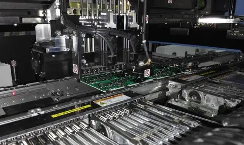
The circuit board manufacturer explains the embedded software of design rule management through online PCB design


