Explanation of component packaging knowLEDge
Because the components must be isolated from the outside world to prevent the corrosion of the Chip circuit caused by impurities in the air, resulting in the decline of electrICal performance. On the other hand, the packaged chip is also easier to install and transport. Because the quality of packaging technology also directly affects the performance of the chip itself and the design and manufacture of the PCB (printed circuit board) connected to it, it is crucial.
An important indicator to measure whether a component packaging technology is advanced or not is the ratio of chip area to packaging area. The closer this ratio is to 1, the better. Main factors to be considered when packaging:
1. The ratio of chip area to package area is close to 1:1 to improve package efficiency;
2. The pins shall be as short as possible to reduce delay, and the distance between pins shall be as far as possible to ensure mutual interference and improve performance;

3. Based on the requirements of heat dissipation, the thinner the package, the better.
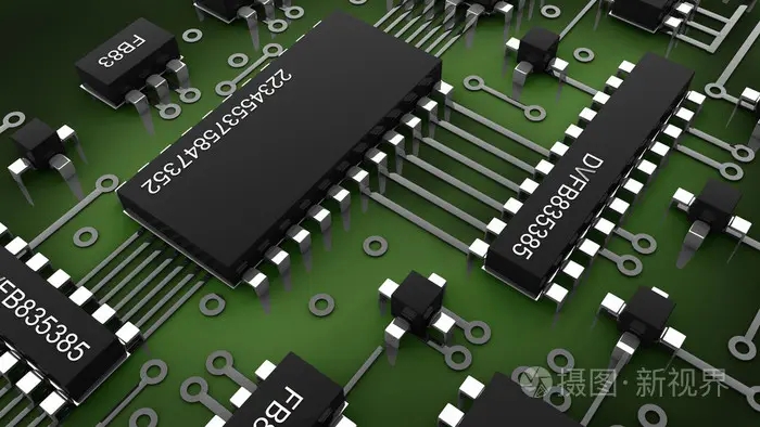
The package is mainly divided into DIP dual in-line package and SMD chip package. In terms of structure, the package developed from the earliest transistor TO (such as TO-89 and TO92) package to the dual in-line package. Later, PHILIP developed the SOP small outline package. Later, SOJ (J-pin small outline package), TSOP (thin small outline package), VSOP (very small outline package), SSOP (reduced SOP), TSSOP (thin reduced SOP) and SOT (small outline transistor) were gradually derived SOIC (small form factor integrated circuit), etc. In terms of materials and media, including metals, ceramics, plastics and plastics, there are still a large number of metal packages for many circuits with high strength working conditions, such as military and aerOSPace.
Packaging has roughly gone through the following development process:
Structure: TO ->DIP ->PLC ->QFP ->BGA ->CSP;
Materials: metal, ceramics ->ceramics, plastics ->plastics;
Pin shape: long lead in line ->short lead or no lead mounting ->spherical bump;
Assembly method: through hole plug-in ->surface assembly ->direct installation
Specific packaging form
1. SOP/SOIC package
SOP is the abbreviation of Small Outline Package, namely Small Outline Package. The SOP packaging technology was successfully developed by Philips from 1968 to 1969. Later, SOJ (J-pin small outline package), TSOP (thin small outline package), VSOP (very small outline package), SSOP (reduced SOP), TSSOP (thin reduced SOP), SOT (small outline transistor), SOIC (small outline integrated circuit), etc. were gradually derived.
2. DIP encapsulation
DIP is the abbreviation of Double In line Package, that is, dual in-line package. One of the plug-in packages, the pins are led out from both sides of the package, and the packaging materials are plastic and ceramic. DIP is the most popular plug-in package, and its application scope includes standard logic IC, memory LSI, microcomputer circuit, etc.
3. PLCC package
PLCC is the abbreviation of Plastic Lead Chip Carrier in English, namely plastic packaging J lead chip package. The PLCC package is square in shape, 32 pin package, with pins all around. The overall dimension is much smaller than that of DIP package. PLCC package is suitable for installing and wiring on PCB with SMT surface mounting technology, and has the advantages of small size and high reliability.
4. TQFP package
TQFP is the abbreviation of thin quad flat package, that is, thin plastic package. The four sided flat pack (TQFP) process can effectively use space, thus reducing the requirements for the space size of printed circuit boards. Due to the reduced height and volume, this packaging process is very suitable for applications requiring high space, such as PCMCIA cards and network devices. Almost all of ALTERA's CPLD/FPGA have TQFP packages.
5. PQFP package
PQFP is the abbreviation of Plastic Quad Flat Package in English, that is, plastic package quad flat package. The distance between the chip pins of PQFP package is very small, and the pins are very thin. Generally, large-scale or very large-scale integrated circuits adopt this package form, and the number of pins is generally more than 100.
6. TSOP package
TSOP is the abbreviation of Thin Small Outline Package, that is, thin small size package. A typical feature of TSOP memory packaging technology is to make pins around the package chip. TSOP is suitable for installing and wiring on PCB (printed circuit board) using SMT technology (surface mounting technology). When TSOP package dimensions are used, parasitic parameters (output voltage disturbance caused by large current changes) are reduced. It is suitable for high-frequency applications, with convenient operation and high reliability.
7. BGA package
BGA is the abbreviation of Ball Grid Array Package, namely ball grid array package. In the 1990s, with the progress of technology, the chip integration has been continuously improved, the number of I/O pins has increased dramatically, the power consumption has also increased, and the requirements for integrated circuit packaging have become more stringent. In order to meet the needs of development, BGA packaging has been applied to production.
The memory packaged with BGA technology can increase the memory capacity by two to three times with the same volume. Compared with TSOP, BGA has smaller volume, better heat dissipation and electrical performance. The BGA packaging technology has greatly improved the storage capacity per square inch. The memory products using BGA packaging technology are only one third of the size of TSOP packaging under the same capacity; In addition, compared with the traditional TSOP packaging, BGA packaging has a faster and more effective way of heat dissipation.
The I/O terminals of BGA package are distributed under the package in the form of circular or columnar solder joints in an array. The advantage of BGA technology is that although the number of I/O pins has increased, the pin spacing has not decreased, but has increased, thus improving the assembly yield; Although its power consumption is increased, BGA can be welded by controllable collapse chip method, which can improve its electrothermal performance; The thickness and weight are reduced compared with the previous packaging technology; The parasitic parameters are reduced, the signal transmission delay is small, and the use frequency is greatly increased; Coplanar welding is available for assembly, with high reliability.
When it comes to BGA packaging, it is necessary to mention Kingmax's patented TinyBGA technology. The full English name of TinyBGA is Tiny Ball Grid Array, which belongs to a branch of BGA packaging technology. It was successfully developed by Kingmax in August 1998. The ratio of chip area to package area is not less than 1:1.14, which can increase the memory capacity by 2 to 3 times with the same volume. Compared with TSOP package products, it has smaller volume, better heat dissipation and electrical performance.
Memory products using TinyBGA packaging technology have a volume of only 1/3 that of TSOP packaging under the same capacity. The pins of TSOP package memory are led out from around the chip, while TinyBGA is led out from the center of the chip. This method effectively shortens the transmission distance of the signal. The length of the signal transmission line is only 1/4 of that of the traditional TSOP technology, so the signal attenuation is also reduced. This not only greatly improves the anti-interference and noise resistance of the chip, but also improves the electrical performance. TinyBGA packaging chip can resist up to 300MHz external frequency, while traditional TSOP packaging technology can only resist up to 150MHz external frequency.
The memory of TinyBGA package is also thinner (package height is less than 0.8mm), and the effective heat dissipation path from the metal substrate to the radiator is only 0.36mm. Therefore, TinyBGA memory has higher heat conduction efficiency, which is very suitable for long running systems with excellent stability.
Packaging and naming rules for some international brand products
1、 MAXIM
MAXIM prefix is "MAX". DALLAS starts with "DS". MAX ××× Or MAX ××××
explain:
1. The suffixes CSA and CWA, where C stands for ordinary level, S stands for surface sticker, and W stands for wide body surface sticker.
2. The suffix CWI means wide body surface sticker, EEWI wide body industrial surface sticker, and the suffix MJA or 883 is military grade.
3. The suffixes of CPA, BCPI, BCPP, CPP, CCPP, CPE, CPD and ACPA are all ordinary dual in-line plug.
For example, MAX202CPE and CPE ordinary ECPE ordinary belt anti-static protection
MAX202EEPE industrial anti-static protection (- 45 ℃ - 85 ℃), indicating that E refers to anti-static protection MAXIM digital arrangement classification
1 prefix simulator;
2-prefix filter;
3-head multiplex switch;
4-head amplifier;
5-head digital to analog converter;
6 prefix voltage reference;
7 prefix voltage conversion;
8-prefix reset device;
9 prefix comparator;


