Some basic requirements of PCB board pad design
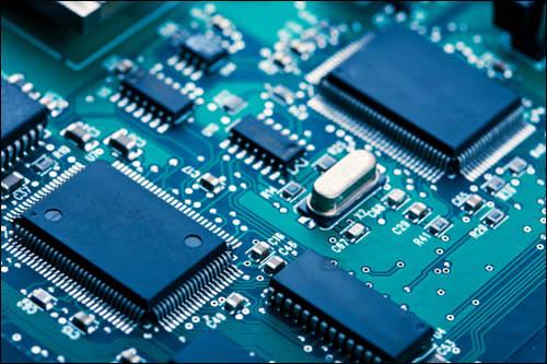
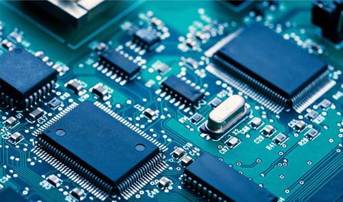
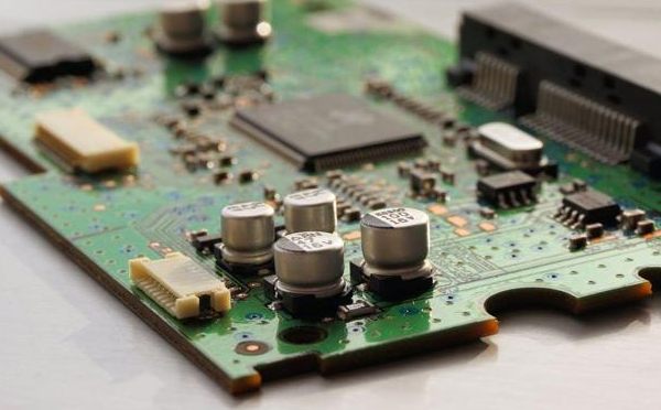
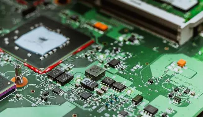
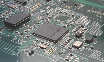
On the printed circuit board, the electrical connection of all components is carried out through the pad. Pad is the most important basic unit in PCB design.


On the printed circuit board, the electrical connection of all components is carried out through the pad. Pad is the most important basic unit in PCB design.
The general PCB basic design process is as follows:Preliminary preparation →PCB structure design → mesh guide → rule setting →PCB layout → Wiring → Routing optimization and silk screen → Network and DRC inspection and structure inspection → light drawing
Double-sided PCB extends from the substrate surface to both sides are composed of line layer, solder resistance layer, character layer, and through the drilling layer through the top bottom line to achieve connected electrical ventilation. In the actual p
Design used to pay attention to the visual effects of the board, now is different. The automatic circuit board design is not as beautiful as the manual design, but the electronic characteristics can meet the requirements, and the complete performance of t

With the PCB design time is shorter and shorter, the size requirements are smaller and smaller, and the device density is higher and higher, the PCB design is more and more difficult. Many manufacturers tend to use special EDA tools to achieve PCB design.
Designing high-speed systems requires not only high-speed components, but also genius and careful design.
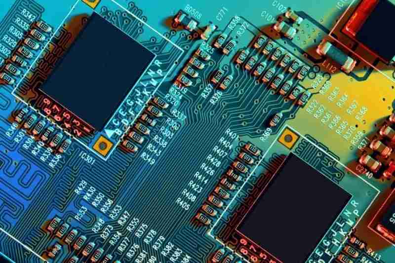
Copper coating has advantages and disadvantages. PCB design for two layer board, high resistance loop, multilayer board (microstrip line), copper coating is very necessary. For multilayer high speed digital circuits with a complete power supply and ground
Although PCB designers can make their own panels, contract manufacturers are generally recommended to carry out this work. Manufacturers collaborate to build and design panels based on size, shape, assembly standards and expected production volumes.
The components should be designed inside the PCB board. The size of the PCB board area and the way of fixing determine the size of the margin around the board. In the whole page to achieve uniform layout, consistent density. Because the wider the printed
PCB design determines the manufacturing, installation and later maintenance costs of printed boards to a certain extent. Excellent PCB routing design can often achieve a higher spread rate, reduce jumper distribution, electromagnetic interference between
PCB design should consider many factors, such as external connection layout, layout design, optimization layout of internal electronic components, etc. The function of PCB design is to standardize the design operation, improve the production efficiency an
Before PCB design, it is necessary to make preliminary preparation, then design structure, layout, wiring, wiring optimization and silk-screen placement, check network DRC and structure, and finally make the board. PCB design is a flawed art, there is no


