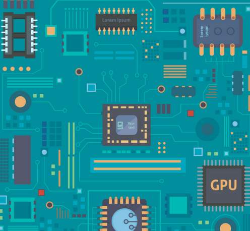
Common wiring rules
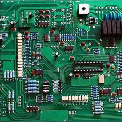
Layout is an important part of design. The result of layout will directly affect the effect of wiring, so it can be considered that a reasonable layout is the first step of successful PCB design.


Layout is an important part of design. The result of layout will directly affect the effect of wiring, so it can be considered that a reasonable layout is the first step of successful PCB design.
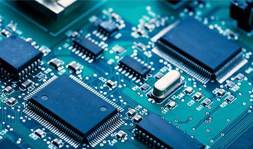
Priority shall be given to the layout of important unit circuits and core components. Routing signal line priority: analog small signal, high-speed signal, clock signal and synchronization signal and other key signals priority wiring.
For some simple products, PCB design may simply connect all the devices and networks accordingly. For high-speed circuit, RF circuit, PCB design directly affects whether the function of the product is normal, whether the product can meet the market requir
Now PCB proofing factories generally provide expedited service, such as 12 hours, 24 hours expedited delivery; Usually the normal delivery time of single and double panels is 2 days.
Therefore, pcb manufacturers believe that when designing or reinforcing equipment, they should be placed on PCB boards with higher hardness, or use certain methods to avoid pcba processing.
The layout should meet the following requirements as far as possible: the overall connection should be as short as possible, and the key signal line should be the shortest; High voltage and high current signals are completely separated from low voltage, l
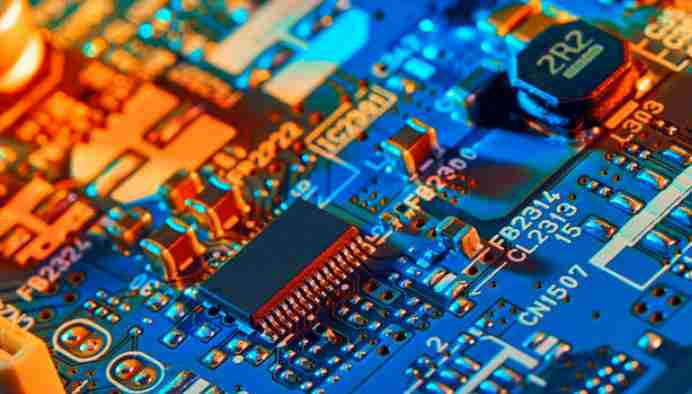
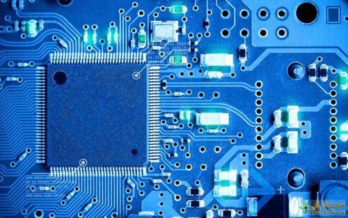
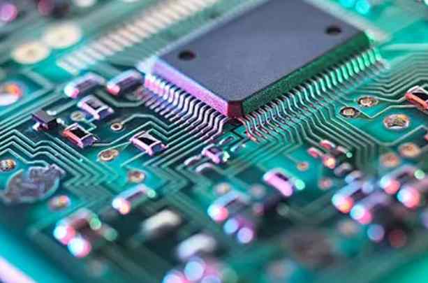
The design of high frequency circuit PCB is a complicated process, which involves many factors, which may directly affect the performance of high frequency circuit.
Wiring is the general requirement of high frequency PCB design on the basis of reasonable layout. Wiring includes automatic wiring and manual wiring.
Both schematic drawing and PCB design should be considered from the high frequency working environment in order to design a more ideal PCB.
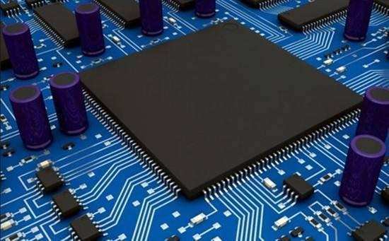
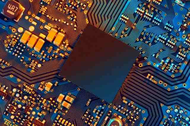
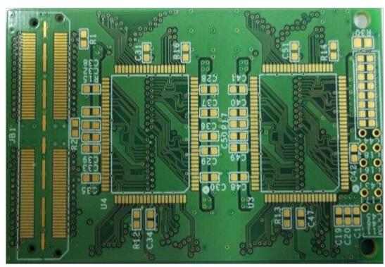
Every hole on PCB is called through hole. From the perspective of function, through hole can be divided into two categories: one is used as an electrical connection between layers; The second is used for fixing or positioning devices. If from the process,
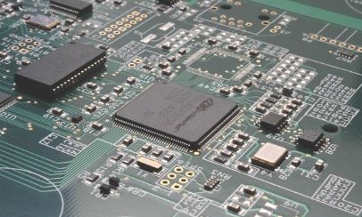
The manufacturing process of PCBA involves many links, and only by controlling the quality of each link can a good product be produced. Generally, PCBA is made of a series of PCB circuit board manufacturing, component purchasing and inspection, SMT patch
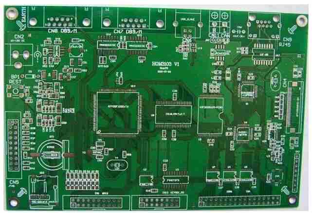
PCB fabrication, of course, refers to the fabrication of the bare printed circuit board itself, while PCB assembly refers to placing components on the printed circuit board.


