Self-study PCB design how to learn
There are three ways to learn PCB well: understand the working principle of components, learn the theoretical basis, and make more boards by hand


There are three ways to learn PCB well: understand the working principle of components, learn the theoretical basis, and make more boards by hand
Metal core board PCBS are not very common in consumer products, and DFM differs little from standard PCBS in other aspects of metal core board PCB design.
As the trend of electronic design continues to evolve, the core elements of functionality, usability and price remain the most important factors for engineers. This has always been CadSoft's strength. CadSoft provides engineers with functional, low-cost s
The difficulty of PCB design is that there are more and more devices with different digital logic, and these circuits with different logic thresholds and voltage swings must be designed together on a PCB multilayer circuit board.
In PCB circuit board design software, it generally includes schematic design and PCB design two modules; Now commonly used software are AltiumProtel series, Altium Designer 6.0, Mentor Graphics PADS series, Cadence OrCAD and P-CAD2006PCB design software.
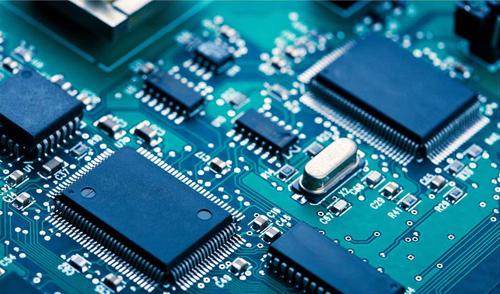
On SMT circuit board, solder joints and components are on the same plane of the circuit board, so in SMT processing PCB, through holes are only used to connect the wires on both sides of the circuit board, the number of holes is much less, and the diamete
The transition to millimetre waves poses a number of challenges for the printed circuit industry, primarily conductor geometry and materials, as the shorter wavelengths reduce the feature size and amplify the relative tolerances inherent in PCB manufactur

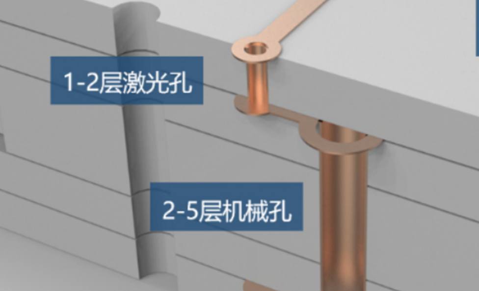
Local peaks and valleys may be produced, resulting in highly irregular effective substrates after pressing. The manufacture of printed circuit boards introduces local differences in etching/plating flow patterns depending on the direction.
pcb circuit board has many unique technical characteristics, in addition to the above aspects, it also has the characteristics of Testability, as well as Assemblability, through this circuit board can better achieve the miniaturization and lightweight e

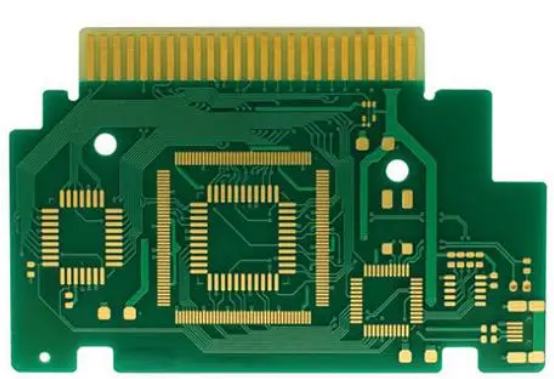
Copper clad plate is the product of glass fiber cloth and copper foil pressed together by epoxy resin and other fusion agents. It is the direct raw material of printed circuit board. It is made into printed circuit board after etching, electroplating and

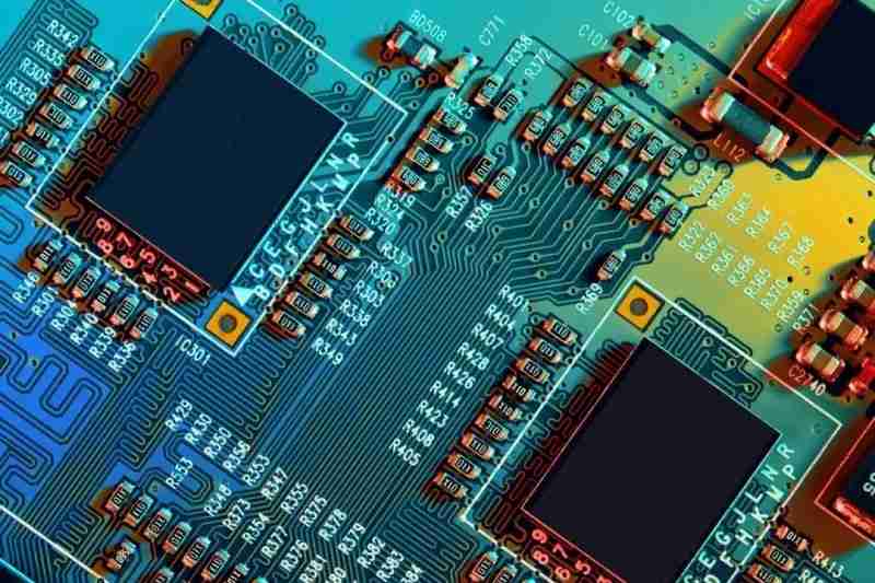
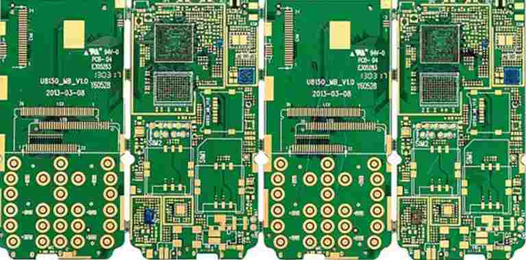
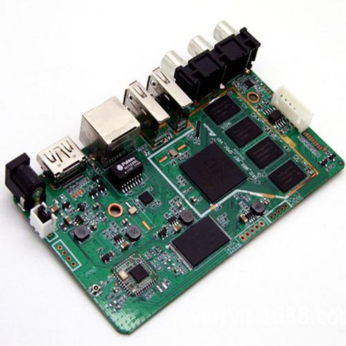
The circuit board is mainly composed of welding pad, through hole, mounting hole, wire, components, connectors, filling, electrical boundary and so on. Common board Layer structures include Single Layer PCB, Double Layer PCB and Multi Layer PCB
To draw simple boards, learn AD. If you want to paint consumer electronics, learn PADS. If you want to draw large boards, follow allegro.


