What are the PCB inspection standards
For PCBS that have been identified as keyboards in the device, these key characteristic parameters and indicators must be centralised and checked from the head in addition to regular inspection. To the toes.


For PCBS that have been identified as keyboards in the device, these key characteristic parameters and indicators must be centralised and checked from the head in addition to regular inspection. To the toes.
the data is also used to check the component function. The data provided by the development department should be as easy as possible to apply directly to the test system or through simple transformations.
Copper coating can not only reduce the ground impedance, but also reduce the cross-sectional area of the loop and enhance the mirror loop of the signal. Therefore, copper coating process plays a very key role in PCB process, incomplete, truncated mirror l

After a lot of practice, the traditional aluminum plug process is changed, and white mesh is used to complete the circuit board surface welding and plug holes. Stable production and reliable quality.
These ground plane planes must be connected to the main ground plane through multiple through-holes. It should be noted that the existence of ground point will cause the inductance characteristics of the side to change, so the selection of inductance valu
From parameters to manufacturers, people who do not understand the specific application scenarios of products, and people who know directly study the cost performance ratio.
scanning acoustic microscope shows its special advantage in nondestructive detection of multilayer high density PCB. And the general obvious explosion plate is only through the visual appearance can be detected.
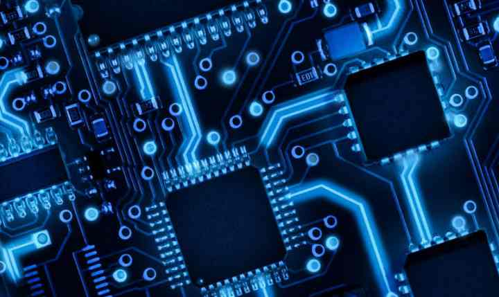
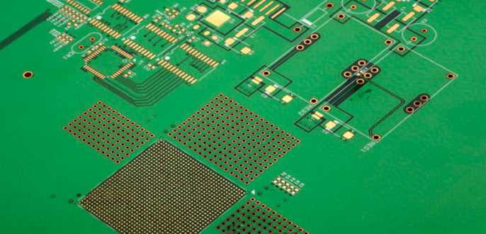
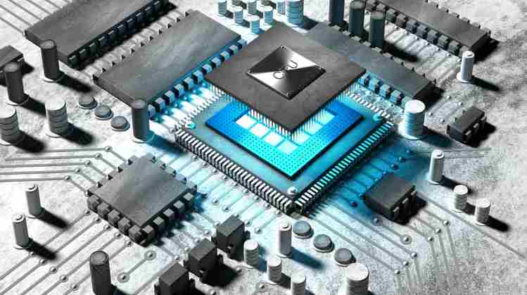
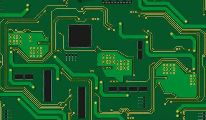
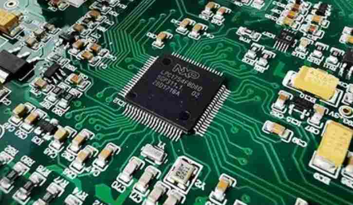
As the carrier of various components and the hub of circuit signal transmission, PCB has become an important and key part of electronic information products. Its quality and reliability level determine the quality and reliability of the whole equipment.
At present, there are more than 100 layers of PCB, then why do people have "PCB multilayer board why are even layers?" What about this question? Relatively speaking, even layer PCB does have more than odd layer PCB.
It should be noted that the simulation design of optical devices to photoelectric conversion (EO\OE), how to accurately reproduce this conversion process in simulation, requires some experience accumulation.
manufacturing technology and system complexity and other key factors have many conflicting requirements, PCB board laminated design is generally considered in various aspects of the key factors after a compromise decision. High - speed digital circuits an

Poor insulation of copper wire will lead to arc between copper wire and copper wire. Too close between the copper trace and the path, it is easy to short-circuit risk; The lack of thickness of the circuit board can lead to bending and breaking.


