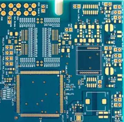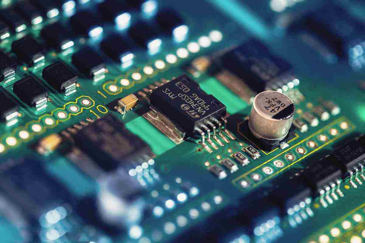
When pcb design matters needing attention complete book
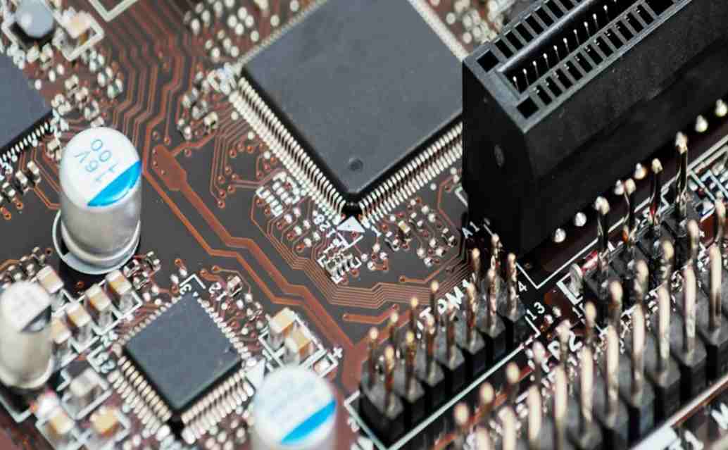
In high-speed logic and circuit design, for some key signals, such as clock, control signals, to add the source end matching resistance, so that the signal will be reflected back from the load end, because the source impedance matching, the reflected sign