PCB board design of the 8 basic principles
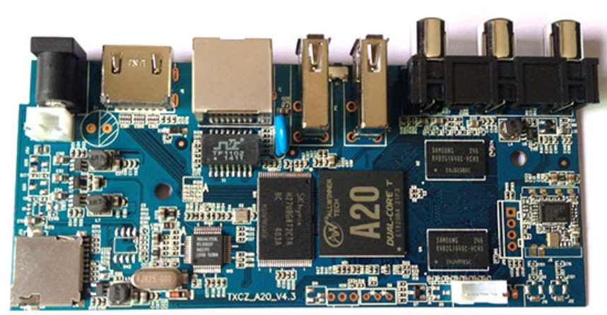
The application of wave-crest welding technology and reflow welding technology are completely different in component layout design, PCB and pad graphic design and hole design.


The application of wave-crest welding technology and reflow welding technology are completely different in component layout design, PCB and pad graphic design and hole design.
Due to the different heat capacity and heating conditions of pad and pin, the temperature to which pad and pin are heated during reflow welding is also different. If the temperature difference is relatively large, it may cause poor welding.
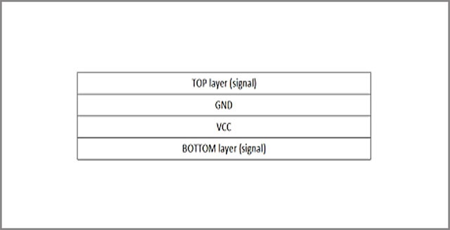
Basic principles of SMB design: layout, wiring, wire width, printed wire spacing, selection of components, selection of PCB substrate, PCB anti-electromagnetic interference, PCB heat dissipation, and arc Angle.
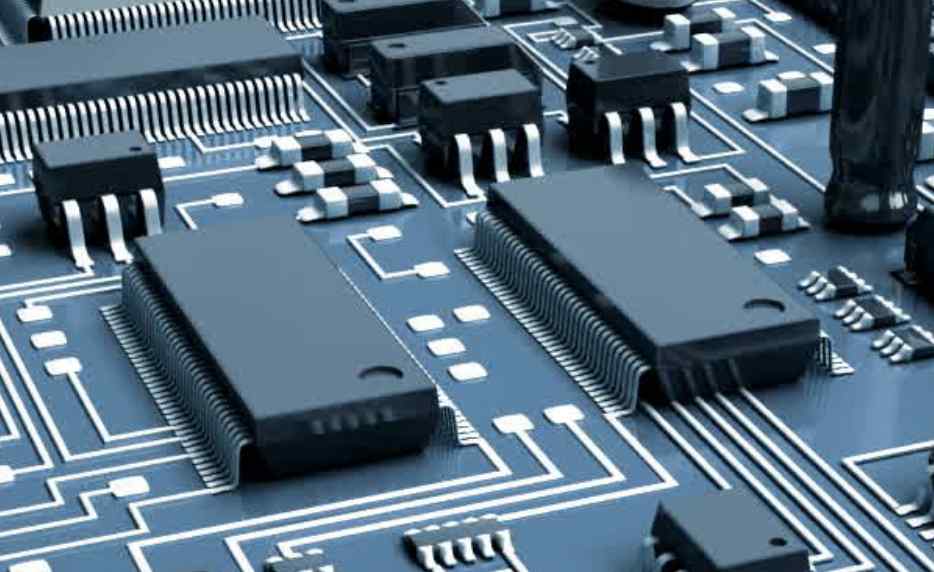
Surface mount technology is very convenient in the manufacture of many PCBS. Reliable and fast professional tools handle installation to ensure that there is no room for human error while speeding up the process.
Common treatment methods are added sewing capacitor and bridge :1, sewing capacitor, 2, bridge, 3, multi-layer wiring, 4, lead bending less, the better, 5, the shorter the better, 6, lead layer alternating less, the better, 7, pay attention to parallel cr
There are the following factors affecting PCB welding quality: PCB diagram, circuit board quality, device quality, device pin oxidation degree, solder paste quality, solder paste printing quality, placement machine programming accuracy, placement machine
PCB design service process: 1. The customer provides schematic diagram to consult PCB design; 2. 2. Evaluate quotation according to schematic diagram and customer design requirements;3. The customer confirms the quotation, signs the contract and pays the
To summarize, the production process of a typical pcb factory is as follows: blanking → inner fabrication → pressing → drilling → copper plating → outer fabrication → soldering paint printing → text printing → surface treatment → contour processing.
The following operations will be carried out in the maintenance technology: 1, inspection of components, 2, welding state analysis, 3, detection of components direction, 4, tool inspection of components, 5, power-on test
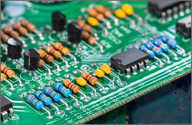
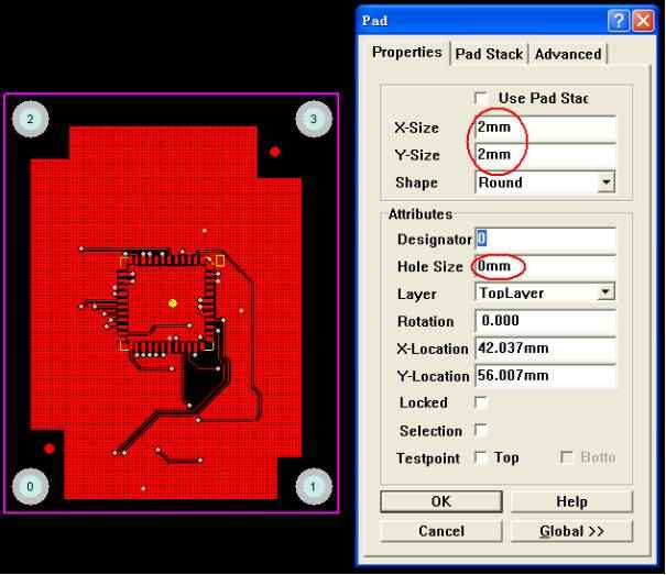
Width and spacing of printed wire are important design parameters, which affect not only the electrical performance and electromagnetic compatibility of PCB, but also the manufacturability and reliability of PCB.
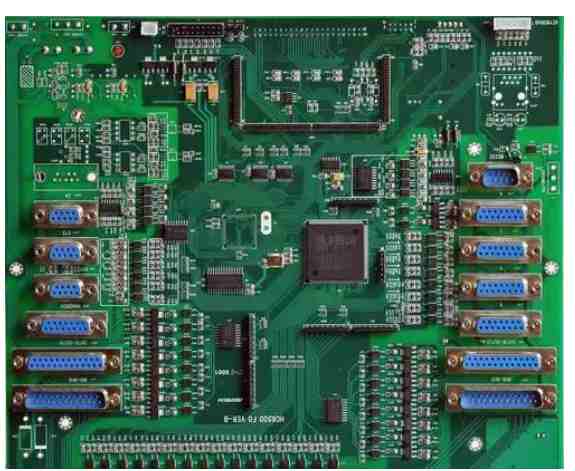
Component layout shall be designed according to SMT electronic processing production equipment and process characteristics and requirements. Different processes, such as reflow welding and wave soldering, have different layouts for components.
To provide you with effective skills to improve PCB design spread rate and design efficiency: 1, determine the number of PCB layers, 2, design rules and restrictions, 3, component layout, 4, fan out design, 5, manual wiring and key signal processing, 6, a


