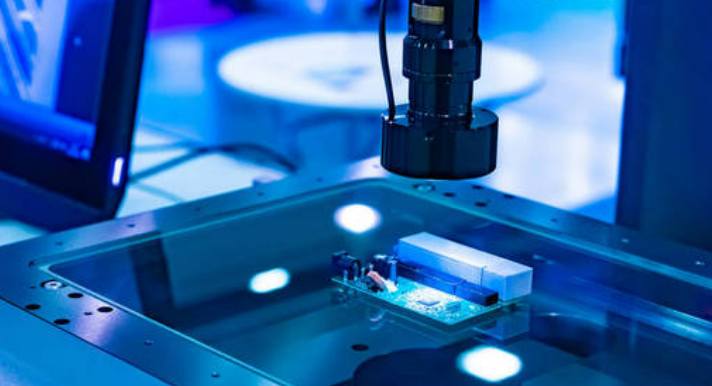
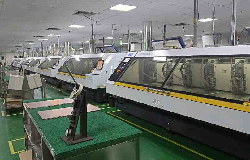
Pre-processing /THT/ hand welding process
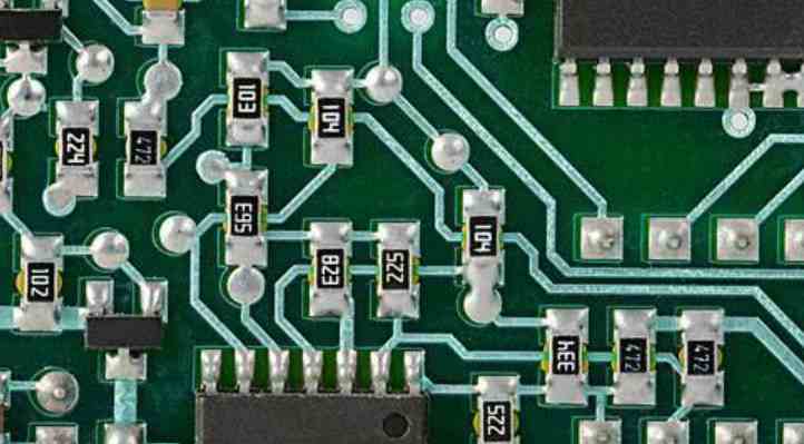
It mainly includes color ring resistor, carbon film resistor, cement resistor, thermistor, varistor, resistor row, variable resistor


It mainly includes color ring resistor, carbon film resistor, cement resistor, thermistor, varistor, resistor row, variable resistor
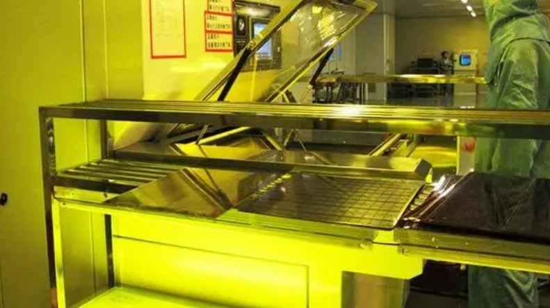
For such a small print, the press must be able to provide an excellent solution to achieve maximum coplanicity between the substrate and the steel mesh.
How to cleverly design multiple circuits of the same circuit structure quickly: 1. Design code segments (code segments), 2. Equipment Table, 3. Multi-channel design method (Multi-channel)
PCB design differential wiring operation skills: 1, activate the wiring instruction, 2, support single line Mode, 3, in the layout of small space position differential wiring, can switch to the Neck Mode, 4, according to the wiring needs to select the app
What is the cause of PCB board broken line: 1, film process: 2, exposure process: 3, development process: 4, etching process: 5, electroplating problem: 6, improper operation

he system speed can be greatly reduced because of the increase of delay time caused by the delay of 2ns per 30cm line length of the common interconnect on the baseboard. Image shift register synchronization counter.
with the increase of labor cost and raw material price again and again, many customers began to require product price reduction to save costs.
In short, the technological parameters and conditions of copper plating must be strictly controlled to ensure that the thickness of the copper plating layer in the hole meets the requirements of the technical standard.
When entering the tin furnace, the liquid tin on the solder plate will be arc shaped by the surface tension of the liquid, resulting in uneven tin thickness on the solder plate.
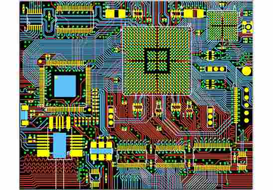
The common multilayer board is generally 4 or 6 layers, complexMultilayer board can reach dozens of layers.
The deformation of the circuit board (PCBA board) usually comes from the rapid temperature rise and rapid temperature drop (thermal expansion and cold contraction) caused by Reflow。
in fact, repair maintenance cost greatly increased at the same time, customer brand affected, It doesn't pay off in the long run.


