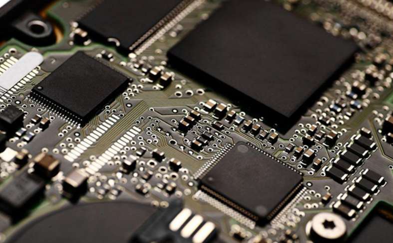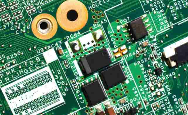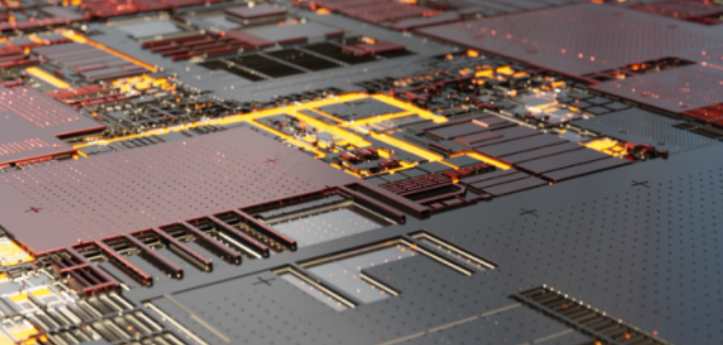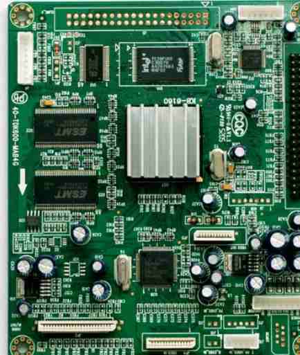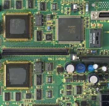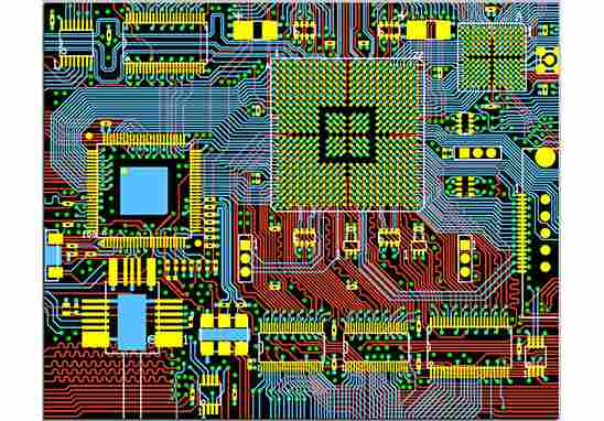
Reliability design of PCB circuit board routing
Width and spacing of printed wire are important design parameters, which affect not only the electrical performance and electromagnetic compatibility of PCB board, but also the manufacturability and reliability of PCB board.